| Home | About Us | Contribute | Bookstore | Advertising | Subscribe for Free NOW! |
| News Archive | Features | Events | Recruitment | Directory |
News
25 July 2010
Output from vertical nitride LEDs boosted by 21%
Researchers at Chonbuk National University and electronic components company LG Innotek in South Korea have been using selective area growth (SAG) to improve the performance of vertical nitride LEDs grown on sapphire, claiming a 21% increase in light output compared with conventional vertical LEDs [Jae Hyoung Ryu et al, Jpn. J. Appl. Phys., vol49, p072102, 2010].
Creating vertical LED structures using nitride semiconductor materials can be difficult since the sapphire substrate is electrically insulating. One can use free-standing gallium nitride or silicon carbide substrates, but these materials are very expensive.
Traditional nitride semiconductor LEDs grown on sapphire have the contacts on the same side of the wafer with non-vertical current flow (Figure 1). These devices also suffer from severe thermal problems since heat degrades LED performance, but heat dissipation through sapphire is very poor.
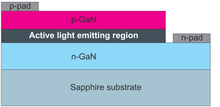 Figure 1. Schematic of traditional non-vertical LED.
Some groups have instead attempted to remove the sapphire substrate after the LED epitaxial layers have been grown. A common technique for this is laser lift-off (LLO). However, this method can introduce new defects, such as dislocation and cracks, which can degrade the performance of the device. Also, the strain structure of the LED layers on sapphire can lead to severe bowing of the wafer (Figure 2).
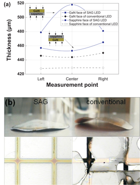 Figure 2. Bowing measurement of GaN LEDs grown by SAG and conventional methods. (b) Photographs showing bowing of LED structures after removal of sapphire substrate.
SAG LED structures were grown on c-plane (0001) sapphire using metal-organic chemical vapor deposition (MOCVD). The GaN template was formed by depositing a 30nm nucleation layer followed by 1μm of undoped and 2.5μm silicon-doped (n-type) GaN. A silicon dioxide (SiO2) mask layer was then grown using plasma-enhanced CVD. Square regions measuring 1000μm x 1000μm were cut out of the SiO2, leaving 90μm mask stripes.
The LED structures were then grown in the windows (Figure 3). The active, light-emitting region consisted of a five-period multi-quantum well (MQW) with InGaN wells and GaN barriers optimized for peak emission at 460nm (blue). Before the MQW, a 2.5μm-thick n-contact layer was deposited. The p-contact was 0.25μm followed by 280nm of the transparent conductor indium tin oxide (ITO). 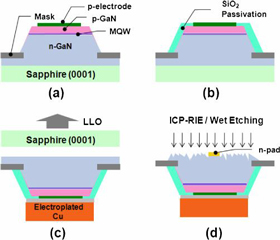
Figure 3. Processing sequence of ridge-shaped vertical LED: (a) growth of p–n junction and p-electrode; (b) passivation of mesa structures by SiO2 deposition; (c) copper electroplating on p-electrode and subsequent removal of sapphire substrate by LLO; and (d) formation of vertical LED chip with textured n-GaN layer.
Electron-beam evaporation was used to deposit a reflecting metal layer on the ITO, followed by an electroplated copper contact. The sapphire substrate was removed using a laser lift-off process with an argon fluoride excimer laser (193nm). The exposed GaN surface was etched down to the n-type material. First an inductively coupled boron tricholoride-chlorine (BCl3/Cl2) plasma reactive ion etch was used and then a wet etch to create a random surface texture. A multi-metal layer was deposited for the n-contact.
A more traditional vertical device was also produced for comparison purposes.
X-ray diffraction studies suggest that the SAG process creates material of ‘almost identical’ quality to that of the template. Also, the wafer bowing of the SAG wafer is ‘significantly relaxed’, compared with the comparison (Figure 2a).
The authors comment: ‘The low bowing of the LED structure grown by SAG is most likely due to the suppression of the lateral strain and dislocations because of the reduction in lateral dimensions, which are difficult to control in conventional growth processes.’
Another improvement is reduced cracking, which often occurs from the strain induced by the wafer bowing. ‘We see no such cracking in SAG LED structures with the ridge geometry,’ the researchers say.
Optical power mapping using a mass-production machine gives a 21% enhancement in power of the bare ridge-shaped SAG LEDs compared with conventional vertical LEDs. The enhancement was 14% for LEDs in molded packaging material. Simulations suggest that some of the enhancement is due to the beveled walls of the SAG LEDs re-directing the light into the surface normal direction for the emitting face of the LED.
See related items:
LG orders four Veeco TurboDisc K465 GaN MOCVD systems
![]() Search: Chonbuk LG Innotek
Search: Chonbuk LG Innotek
Visit: http://jjap.ipap.jp/link?JJAP/49/072102
Visit: www.lginnotek.com/main.jsp
The author Mike Cooke is a freelance technology journalist who has worked in the semiconductor and advanced technology sectors since 1997.
![]() ©2010 Juno Publishing and Media Solutions Ltd. All rights reserved. Semiconductor Today and the editorial material contained within it and related media is the copyright of Juno Publishing and Media Solutions Ltd. Reproduction in whole or part without permission from Juno Publishing and Media Solutions Ltd is forbidden. In most cases, permission will be granted, if the author, magazine and publisher are acknowledged.
©2010 Juno Publishing and Media Solutions Ltd. All rights reserved. Semiconductor Today and the editorial material contained within it and related media is the copyright of Juno Publishing and Media Solutions Ltd. Reproduction in whole or part without permission from Juno Publishing and Media Solutions Ltd is forbidden. In most cases, permission will be granted, if the author, magazine and publisher are acknowledged.
Disclaimer: Material published within Semiconductor Today and related media does not necessarily reflect the views of the publisher or staff. Juno Publishing and Media Solutions Ltd and its staff accept no responsibility for opinions expressed, editorial errors and damage/injury to property or persons as a result of material published.
Semiconductor Today, Juno Publishing and Media Solutions Ltd, Suite no. 133, 20 Winchcombe Street, Cheltenham, GL52 2LY, UK
Web site by No Name No Slogan ![]()