| Home | About Us | Contribute | Bookstore | Advertising | Subscribe for Free NOW! |
| News Archive | Features | Events | Recruitment | Directory |
News
27 January 2010
Creating optical memories from whispers in InP disk lasers on SOI
Photonics researchers have used heterogeneous integration of indium phosphide (InP) onto silicon-on-insulator (SOI) wafers to create an all-optical flip-flop (AOFF) memory aimed at 1.55μm wavelength optical communications [Liu Liu, Nature Photonics, published online 24 January 2010]. The laser power was provided by electrical pumping.
The research was carried out at the INTEC laboratory at Ghent University associated with the European IMEC research center. Eight members of the team were based at INTEC when the research was carried out; two came from the COBRA Research Institute of the Technische Universiteit Eindhoven, and one from the Institut des Nanotechnologies de Lyon, Université de Lyon.
Two competing whispering gallery modes that circulated clockwise (CW) and counter-clockwise (CCW) in InP-based disk laser were used to provide the memory states (Figure 1). Traditional ‘whispering galleries’ are architectural phenomena where whispers can be heard clearly at other locations, particularly under domes in palaces, churches, mosques, Taoist temples, railway stations, etc. Microtechnologists have in recent years produced light analogs of such structures in many material systems.
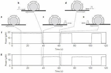
Figure 1: Flip-flop operation and measured laser power at slow switching speeds.
Optical memory devices are seen as vital parts of future high-speed, low-power-consumption photonic integrated circuits that will provide all-optical signal-buffering, switching and processing.
“The total power consumption and the device size are, to the best of our knowledge, the smallest reported to date at telecom wavelengths,” comment the authors. “This is also the only electrically pumped, all-optical flip-flop on silicon built upon complementary metal-oxide semiconductor technology.” Alternative approaches include using delay lines or converting the optical signal into electronic memory. However, these techniques can be complex, bulky and/or power hungry (Table 1).
Device size |
Electrical bias current |
Switching energy |
Switching speed |
Material system |
|
μm |
mA |
fJ |
ps |
||
Coupled ring laser |
2x16x16 |
>2x30 |
5.5 |
20 |
lnP |
Single ring laser |
>50x50 |
>60 |
4 |
130 |
lnP |
VCSEL |
10x10 |
14.5 |
1.8 (50MHz)/ 10 (3.1GHz) |
300 |
lnP |
INTEC’s microdisk laser |
7.5x7.5 |
3.5 |
1.8 |
60 |
lnP on SOl |
Table 1: Comparison of proposed AOFFs, including research reported here (last line).
 The researchers feel that their AOFF memory for a moderate number of bits (from a few to hundreds) could be translated into a practical product for optical packet or packet header processing in the near future. Larger numbers of AOFF memory elements “is still complex and probably a long way from realization.”
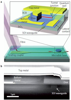
Figure 2: Schematic and SEM image of microdisk laser memory on SOI wafer.
The researchers used divinylsiloxane–benzocyclobuten (DVS–BCB) polymer adhesive to bond 7.5μm diameter InP-based disk lasers to SOI wafers (Figure 2). The laser structure was 583nm thick and consisted of three compressively strained layers of indium arsenide phosphide (InAsP) on InP. A tunnel junction was used to provide a low-loss p-type contact. This unpatterned InP-based structure was flipped and bonded to the SOI wafer. The InP substrate was then removed.
Once the laser material was applied to the SOI, contact lithography was used to define the laser disks. Inductively coupled plasma reactive ion etch (ICP-RIE) was performed to create the disks on top of a thin lateral n-type InP layer on which the bottom contact was deposited. The disk laser was covered with DVS-BCB and then a via formed for the top contact. The whispering gallery modes are confined to the edge of the disk so the top contact does not block access from the external light sources that set the mode direction (CW/CCW). The memory state is read and set through two 500nm x 220nm SOI waveguides. Since the SOI wafer is a poor thermal conductor, a gold layer was used as a heat sink to reduce the thermal resistance to 6.1K/mW from the 10K/mW of previous work with InP lasers on SOI.
The device operates in continuous-wave mode and consumes about a few millwatts. Mode switching was achieved at speeds as low as 60ps (6x10-11 seconds), consuming 1.8fJ (1.8x10⁻¹⁵J) to make the change. The researchers believe that this speed is adequate for 10Gb/s optical communication data rates. Further speed optimization of the disk should enable 40Gb/s performance with an energy consumption that is ‘very competitive’ with standard silicon CMOS-based memory solutions.
![]() Search: InP SOI wafers
Search: InP SOI wafers
Visit: www2.imec.be
Visit: http://dx.doi.org/10.1038/NPHOTON.2009.268
The author Mike Cooke is a freelance technology journalist who has worked in the semiconductor and advanced technology sectors since 1997.
![]() ©2010 Juno Publishing and Media Solutions Ltd. All rights reserved. Semiconductor Today and the editorial material contained within it and related media is the copyright of Juno Publishing and Media Solutions Ltd. Reproduction in whole or part without permission from Juno Publishing and Media Solutions Ltd is forbidden. In most cases, permission will be granted, if the author, magazine and publisher are acknowledged.
©2010 Juno Publishing and Media Solutions Ltd. All rights reserved. Semiconductor Today and the editorial material contained within it and related media is the copyright of Juno Publishing and Media Solutions Ltd. Reproduction in whole or part without permission from Juno Publishing and Media Solutions Ltd is forbidden. In most cases, permission will be granted, if the author, magazine and publisher are acknowledged.
Disclaimer: Material published within Semiconductor Today and related media does not necessarily reflect the views of the publisher or staff. Juno Publishing and Media Solutions Ltd and its staff accept no responsibility for opinions expressed, editorial errors and damage/injury to property or persons as a result of material published.
Semiconductor Today, Juno Publishing and Media Solutions Ltd, Suite no. 133, 20 Winchcombe Street, Cheltenham, GL52 2LY, UK
Web site by No Name No Slogan ![]()