| Home | About Us | Contribute | Bookstore | Advertising | Subscribe for Free NOW! |
| News Archive | Features | Events | Recruitment | Directory |
News
8 February 2010
Germanium lines up bands for laser action
Researchers in the Electronic Materials Research Group at Massachusetts Institute of Technology (MIT) have manufactured a direct energy bandgap in germanium (Ge) on silicon (Si) [Jifeng Liu et al, Optics Letters, published online 26 January 2010], enabling construction of what is claimed to be the first room-temperature laser emitting at infrared wavelengths of about 1600nm (1.6μm). This falls in the L band for fiber-optic communication systems (1565–1625nm). The conventional C-band is a little shorter, at 1530–1565nm.
The hope is that MIT’s technology will provide an easier route to integration of lasers and mainstream electronics, since germanium is already used in CMOS processes.
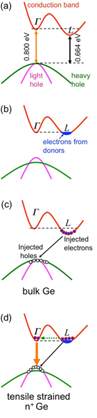 Figure 1: (a) Electrons can be excited from the valence band (green) to the conduction band (red), allowing free movement around the crystal. In the conduction band, electrons quickly adopt the lowest-energy states (right-hand well). In an indirect-bandgap material like germanium, the crystal momentum of the lowest-energy state is misaligned with that of the valence band (yellow and black arrows), so the electron will not emit a photon when it loses energy.
(b) MIT researchers fill up the lower-energy state with extra electrons from phosphorous atoms, which they add to the germanium.
(c) When an electron is excited into the conduction band, it leaves behind a ‘hole’ in the valence band. The researchers inject pairs of electrons and holes into the germanium.
(d) When the injected electrons find the lower-energy state occupied, they spill over into the other direct state; realigned with the holes, they release their extra energy as photons.
Normal germanium is ruled out as a useful laser material since its bandgap is indirect — meaning that the valley of the conduction band does not line up with the peak of the valence band in the electron wave-vector (k) space (Figure 1). Simple transitions creating light can only change wave-vector by an amount of the order the wave-vector of the light (~1/wavelength) — a value that is effectively zero for visible light (~2x10⁻⁴/Å), and even smaller for infrared (~1x10⁻⁴/Å), compared with the wave-vector range deriving from the crystal lattice (~1/lattice spacing, ~0.2/Å).
MIT has been working for a while on how to create a direct bandgap in germanium. Theoretical work reported in 2007 suggested that tensile strain and n-type doping could achieve this. Since then, direct-gap photoluminescence and optical gain at room temperature have been demonstrated.
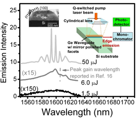 Figure 2: Edge emission spectra of Ge waveguide with mirror polished facets under 1064nm excitation from a Q-switched laser (spectral resolution of measurement, 2nm). Three spectra at 1.5, 6.0 and 50μJ/pulse pumping power correspond to spontaneous emission, threshold for lasing, and laser emission, respectively. Inset: cross-sectional SEM of Ge waveguide and schematic of experimental setup for optical pumping.
Now, an edge-emitting waveguide lasing device has been created using tensile-strained n+-doped Ge. The Ge waveguide layers were grown selectively on the silicon wafer using ultra-high-vacuum chemical vapor deposition (UHVCVD) with silicon dioxide used as a mask (Figure 2). The 0.24% tensile strain was introduced through cooling the Ge to room temperature from a relaxed state at 650°C. This reduces the direct gap to 0.76eV, while the indirect gap is normally about 0.66eV. In-situ doping with 1x10¹⁹/cm3 phosphorus compensated for the remaining difference. It is hoped in future to increase even further the level of doping, increasing power efficiency.
The lasing was shown through optical pumping (Figure 2) with excitation by a Q-switched laser emitting 1064nm radiation (1.5ns pulse, 50μJ/pulse, 1kHz repetition).
Funding for the project comes from the Si-Based-Laser Initiative of the Multidisciplinary University Research Initiative (MURI), sponsored by the Air Force Office of Scientific Research (AFOSR).
![]() Search: MIT Germanium laser Germanium
Search: MIT Germanium laser Germanium
Visit: http://photonics.mit.edu
The author Mike Cooke is a freelance technology journalist who has worked in the semiconductor and advanced technology sectors since 1997.
![]() ©2010 Juno Publishing and Media Solutions Ltd. All rights reserved. Semiconductor Today and the editorial material contained within it and related media is the copyright of Juno Publishing and Media Solutions Ltd. Reproduction in whole or part without permission from Juno Publishing and Media Solutions Ltd is forbidden. In most cases, permission will be granted, if the author, magazine and publisher are acknowledged.
©2010 Juno Publishing and Media Solutions Ltd. All rights reserved. Semiconductor Today and the editorial material contained within it and related media is the copyright of Juno Publishing and Media Solutions Ltd. Reproduction in whole or part without permission from Juno Publishing and Media Solutions Ltd is forbidden. In most cases, permission will be granted, if the author, magazine and publisher are acknowledged.
Disclaimer: Material published within Semiconductor Today and related media does not necessarily reflect the views of the publisher or staff. Juno Publishing and Media Solutions Ltd and its staff accept no responsibility for opinions expressed, editorial errors and damage/injury to property or persons as a result of material published.
Semiconductor Today, Juno Publishing and Media Solutions Ltd, Suite no. 133, 20 Winchcombe Street, Cheltenham, GL52 2LY, UK
Web site by No Name No Slogan ![]()