| Home | About Us | Contribute | Bookstore | Advertising | Subscribe for Free NOW! |
| News Archive | Features | Events | Recruitment | Directory |
News
9 February 2010
Kyma and RPI search m-plane GaN for LED wavelength stability
Rensselaer Polytechnic Institute (RPI) and Kyma Technologies have been using m-plane gallium nitride (GaN) substrates to improve the wavelength stability of cyan and green light-emitting diodes (LEDs) [Theeradetch Detchprohm et al, Appl. Phys. Lett., vol96, p051101, 2010]. It is hoped that more efficient, better-quality white-light emission units will ultimately be created by combining light from red, green and blue (RGB) LEDs.
Presently, most ‘white’ LEDs consist of a blue LED and a yellow phosphor material that absorbs some of the blue light and re-emits over a broad range of wavelengths around yellow to give an approximation to white light. Although this is the most commercial process (i.e. low cost) at the moment, it has two main drawbacks: a loss of energy in the re-emission that naturally leads to lower efficiency; and, poor white color rendering from the limitations of combining blue LED light and yellow phosphorescence.
With an RGB approach, one can hope to attain efficacies as high as 347 lumens per watt (lm/W) and a color rendering index (CRI) of 91. By contrast, blue-phosphor LEDs have reached 161lm/W at 350mA in 1mm2 devices (249lm/W at 20mA). Commercial CRIs vary from around 70 to 85, although Philips Lumileds has one product at 90 that operates at lower efficacy (63lm/W, rather than 100lm/W for a CRI of 70).
While there are well-developed technologies for red and blue LEDs, high-efficacy green LEDs continue to suffer from a number of problems. Attempts to create green LEDs have centered on extending the technology used to make blue (440–490nm) LEDs: indium gallium nitride (InGaN) quantum wells. However, as one moves to the longer green wavelength (520–570nm), one encounters such effects as ‘efficiency droop’ at higher currents and shifts of wavelength with power output.
The polarization properties of the InGaN material are thought to be the source of some of these difficulties. In general, the III-V semiconductors are more ionic in their bonding properties compared with the covalently bonded group IV materials silicon and germanium. For InGaN, the nitrogen (group V) tends to be more negatively charged, while the indium and gallium (group III) tend to be more positively charged. This leads to spontaneous polarization; when strain is introduced, the polarization changes and creates piezoelectric effects.
These polarization effects can be mitigated or even eliminated by using substrates where the GaN crystal structure is oriented in a different direction from the normal c-plane surface [0001]. The m-plane [10-10] has a vanishing polarization. There is a cost to using non-standard, less mature materials: some approaches to creating m-plane substrates introduce high densities of threading dislocations and crystal stacking faults that can limit device performance.
Kyma prepared the m-plane substrates for the RPI work by cutting c-axis GaN crystal boules that were grown using hydride vapor phase epitaxy (HVPE). The substrates were 0.5mm x 5mm x 10mm. Chemo-mechanical polishing (CMP) was used to achieve atomic flatness with root mean square roughness less than 0.5nm. The surface was slightly miscut: less than 0.2° towards the a-axis and less than 1° towards the c-axis. Such miscutting can improve the crystal quality of subsequently deposited epitaxial layers.
A variety (Table 1) of undoped multi-quantum wells (MQWs) were grown using metal-organic chemical vapor deposition (MOCVD). Some were subjected to photoluminescence (PL) characterizations, while others were built into full LEDs for electroluminescence (EL) experiments. For the LEDs, a silicon-doped n-GaN layer (500nm) was grown before the MQW structure; the LED capping consisted of an Mg-doped p-AlGaN electron blocker (20nm), p-GaN (100nm) and
p+-GaN (20nm). The MQW barriers were 24–26nm thick GaN layers.
Sample |
Type |
x |
Well thickness |
Emission wavelength |
% |
nm |
nm |
||
A |
MQW |
10.0 |
4.4 |
456 ±2 |
B |
MQW |
12.5 |
3.9 |
487 ±2 |
C |
MQW |
15.0 |
4.8 |
512 ±6 |
D |
LED |
16.3 |
4.2 |
483 ±1 |
E |
LED |
19.0 |
4.1 |
489 ±1 |
F |
LED |
17.1 |
4.2 |
492 ±1 |
G |
LED |
18.6 |
4.6 |
516 ±3 |
Table 1: Summary of m-plane InxGa1-x/GaN MQW and LED samples; peak PL wavelength for MQW and dominant EL wavelength for LED.
One disadvantage of using m-plane substrates for long-wavelength LEDs is that piezoelectric polarization fields give a red-shift (Stokes shift), extending the wavelength for more traditional c-plane substrate LEDs. For long-wavelength m-plane LEDs, one either needs to have higher indium concentrations, wider wells, or both. Higher-indium-concentration InGaN is difficult to grow with high quality, since the lattice mismatch with GaN is greater.
The longer-wavelength LEDs showed increasing efficiency droop and lower light output power (Figure 1). The linewidths of both MQWs and LEDs were around 150meV (~30nm in wavelength terms). In compensation, the blue-shift in wavelength was just 3nm in moving from current densities of 0.3A/cm2 to 38A/cm2. This compares with c-plane device blue-shifts of 5nm for a 484nm wavelength and 24nm for 510nm.
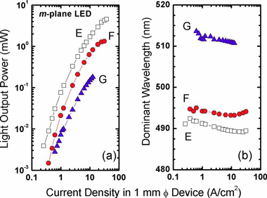
Figure 1: Current-dependent EL characteristics of m-plane cyan and green GaInN/GaN LEDs: partial light output power (LOP) (a) and dominant wavelength (b).
The paper comments: ‘This blueshift is typically attributed to the partial screening of piezoelectric charges across the GaInN/GaN QWs, which increases with InN fraction in polar c-plane LEDs. Here, however, we find evidence that such color shift in cyan and even green LEDs can be avoided with nonpolar m-plane growth.’
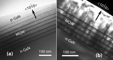
Figure 2: Cross-sectional TEM micrographs of m-plane LEDs with dominant wavelength of 483nm (a, sample D) and 516nm (b, sample G).
Transmission electron microscopy (TEM) of the LEDs was used to investigate possible causes for the drop-off in efficiency at longer wavelengths. Sample D, a cyan/483nm LED, was found to contain no threading dislocations in addition to those emanating from the substrate (nominally less than 5x10⁶/cm2). However, misfit dislocations were found in the longer-wavelength cyan/492nm LED F. For the longest-wavelength LED (516nm), G, the threading dislocation density was of the order of 1010/cm2.
See related items:
Kyma wins $2.8m DoD funding for low-defect GaN development
InGaN LED spillover and efficiency droop
Kyma completes custom crystal fabrication facility
![]() Search: Rensselaer Polytechnic Kyma GaN substrates Green LEDs
Search: Rensselaer Polytechnic Kyma GaN substrates Green LEDs
Visit: http://link.aip.org/link/?APPLAB/96/051101/1
The author Mike Cooke is a freelance technology journalist who has worked in the semiconductor and advanced technology sectors since 1997.
![]() ©2010 Juno Publishing and Media Solutions Ltd. All rights reserved. Semiconductor Today and the editorial material contained within it and related media is the copyright of Juno Publishing and Media Solutions Ltd. Reproduction in whole or part without permission from Juno Publishing and Media Solutions Ltd is forbidden. In most cases, permission will be granted, if the author, magazine and publisher are acknowledged.
©2010 Juno Publishing and Media Solutions Ltd. All rights reserved. Semiconductor Today and the editorial material contained within it and related media is the copyright of Juno Publishing and Media Solutions Ltd. Reproduction in whole or part without permission from Juno Publishing and Media Solutions Ltd is forbidden. In most cases, permission will be granted, if the author, magazine and publisher are acknowledged.
Disclaimer: Material published within Semiconductor Today and related media does not necessarily reflect the views of the publisher or staff. Juno Publishing and Media Solutions Ltd and its staff accept no responsibility for opinions expressed, editorial errors and damage/injury to property or persons as a result of material published.
Semiconductor Today, Juno Publishing and Media Solutions Ltd, Suite no. 133, 20 Winchcombe Street, Cheltenham, GL52 2LY, UK
Web site by No Name No Slogan ![]()