- News
3 December 2010
Corning probes optical losses in nitride laser at wafer-level
Corning Inc has developed a method to assess the internal optical waveguide loss of laser diode (LD) wafers at an earlier stage in the development process, compared with alternative techniques [Dmitry S. Sizov et al, Appl. Phys. Express, vol3, p122104, 2010].
Typically waveguide losses are found by creating laser cavities of varying length. The Corning method instead works with wafers before such cavities have been constructed (usually by some plasma etch process). The waveguide losses increase threshold currents, and reduce differential and wall-plug efficiencies.
The method (Figure 1) consists of exciting the material with a laser spot and measuring the photoluminescence at the edge of the wafer. By varying the position of the spot, the optical loss coefficient can be determined, by assuming an approximate 1/R dependence of the light intensity as expected for two-dimensional radiation confined to the waveguide layers. The researchers find that the 1/R approximation is good (i.e. non-confined transmission is negligible) for values of R (distance from spot to wafer edge) of more than 0.1mm and optical losses less than 100/cm.
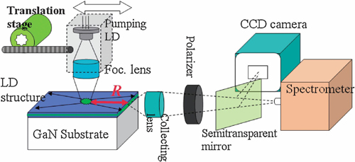
Figure 1: Schematic of internal optical loss measurement setup.
The method’s accuracy depends on ‘bandtail’ states that re-emit photons with energy below the absorption band edge of the system. Nitride semiconductor quantum well (QW) laser diodes constitute such systems with deep bandtails, giving Stokes shifts (i.e. red-shifts) of more than 100meV.
The Corning group applied its technique to blue to green laser diode wafers built on both c-plane and semipolar free-standing gallium nitride (GaN) substrates. The wafers, when formed into laser diodes, produced laser emissions in the wavelength range 480–525nm. The photoluminescence was created using 405nm blue laser diodes (as used in commercial HD DVD and Bluray optical storage systems).
A wafer for ‘aquamarine’ laser diodes (with a lasing wavelength of 497nm) was found to have an optical loss in the waveguide less than 2/cm before activation of the magnesium (Mg) doping used to create the hole injection p-type region of the device (Figure 2). The optical loss up to 520nm is attributed to the QW active region. Longer than 520nm (the QW absorption edge), the losses are attributed to light leakage from the guide and absorption by the guide material. As the wavelength gets longer, the confinement into the waveguide weakens. The 2/cm loss figure for the waveguide is obtained by a suitable extrapolation back to the lasing frequency.
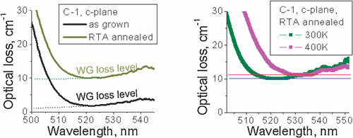
Figure 2: Optical losses of c-plane LD structure before and after p-type activation by RTA (a) and measured at 300K and 400K (b).
However, this loss is before activation of the p-type layer that is needed for such a device to operate as a laser diode. Before the activation, the Mg atoms are associated with hydrogen in complexes that make the material insulating. These complexes were removed by the Corning team using a conventional rapid thermal anneal (RTA) process in an oxygen/nitrogen atmosphere. The effect of this was to increase the optical losses of the waveguide structure to 8–9/cm. These compare with internal optical losses of more than 10/cm that have been published for state-of-the-art blue–green LDs.
The increase in optical losses consequent on activation is attributed to the p-type layer. This was confirmed in experiments where annealing was carried out on structures without Mg doping, where no increase in the optical loss coefficient was observed.
Although Mg doping is the most commercial technique for producing p-type layers in nitride semiconductor structures, it leaves much to be desired. In particular, the activation energy for holes to be released from the Mg acceptors (140–210meV in GaN) is high compared with typical thermal energies (~26meV at 300K, ‘room temperature’). This means that the free hole concentration is about two orders of magnitude lower than the bound hole level (even at 400K).
Increasing the temperature of the structure to 400K only increased the loss slightly – the researchers comment: “Within the measurement accuracy there is no difference in waveguide loss between these two temperatures apart from the QW absorption edge shifting to longer wavelengths due to temperature-induced bandgap shrinkage”. The researchers put their measurement error as being of the order of 1/cm.
Since the increase in temperature should increase the number of free holes significantly, the researchers come to the conclusion that they do not contribute significantly to the waveguide loss. Rather, it is the Mg-bound holes that dominate this behavior.
The researchers obtained similar loss results for structures grown on semipolar gallium nitride substrates. In the c-plane case, only transverse electric (TE) modes of the waveguide were considered to be important. In the semipolar case, modes with different electric field directions occur in waveguides. However, the losses within these modes fell within 2/cm of each other (with the TE mode propagating in the [0001] direction being highest), close to the measurement error.
The work underlines the well-known fact that Mg doping to obtain p-type conductivity in GaN is one of the weakest points of the nitride semiconductor application equation. Finding a method to lower ionization energies for holes to be released from nitride acceptors would reduce optical losses, among many other benefits.
http://apex.jsap.jp/link?APEX/3/122104
The author Mike Cooke is a freelance technology journalist who has worked in the semiconductor and advanced technology sectors since 1997.