| Home | About Us | Contribute | Bookstore | Advertising | Subscribe for Free NOW! |
| News Archive | Features | Events | Recruitment | Directory |
News
24 August 2010
Texas Tech ‘significantly’ improves InGaN solar cell performance
Texas Tech University scientists have developed an indium gallium nitride (InGaN) solar cell with characteristics ‘significantly higher’ than previously reported values for devices with similar indium content in the QWs (~35%) [R. Dahal et al, Appl. Phys. Lett., vol97, p073115, 2010].
Theoretically, nitride semiconductors should be able to extract light over the range of energy bandgaps from indium nitride (InN, ~0.65eV) through gallium nitride (GaN, ~3.4eV) to aluminum nitride (AlN, ~6.2eV). This covers wavelengths from infrared and visible to ultraviolet (2000–200nm). One could envisage a series of different nitride solar cells designed to extract most efficiently a range of different wavelengths.
Even for single cells, one could tune a photovoltaic cell that could achieve better than 50% solar energy conversion by using InGaN alloy with 40% indium fraction. Unfortunately these remain theoretical hopes because it is very difficult to grow high-quality InGaN with high indium contents. The problem is that the lattice mismatch between InN and GaN is high (~11%). Layers with appreciable indium contents tend to segregate into regions with high and low indium content (phase separation). This is one of the difficulties that have hindered the extension of nitride light-emitting technology to longer wavelengths.
Despite the difficulties, university groups across the world are developing nitride semiconductors for use in solar cells. In 2009, the US company RoseStreet Energy Labs Inc announced a tandem nitride–silicon solar cell.
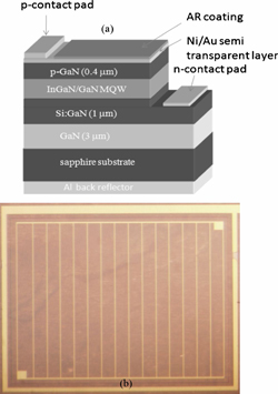 The Texas researchers used a 12-period multi-quantum well (MQW) structure consisting of InGaN/GaN (3nm/16nm) with the In content of the well targeted at 35% (Figure 1). The layers were deposited by metal-organic chemical vapor deposition (MOCVD) on sapphire. The wavelength of the electroluminescence from the structure was around 533nm (green).
Figure 1: (a) Layer structure of InGaN/GaN solar cells with 12 periods of 3nm-thick InxGa1−xN (x approximately 0.35) QW and 17nm GaN barrier, and (b) optical microscopy image of a fabricated solar cell with 2.3mm x 2mm mesa size.
The devices were created by first depositing a semi-transparent layer of nickel/gold by electron-beam evaporation. Then the 2.3mm x 2mm mesas were formed using chlorine-based inductively coupled plasma etch. The semi-transparent p-contact was annealed to give an ohmic characteristic. A nickel-gold grid electrode (6μm wide, 170μm) was deposited on the mesa. The n-contact consisted of titanium/aluminum/nickel/gold. A 100nm silicon dioxide anti-reflection coat was added with plasma-enhance chemical vapor deposition (PECVD). The contact windows were opened in the SiO2 using a wet etch. The sapphire substrate was coated with aluminum to provide a back-reflector.
The device was tested under standard 1.5 air mass (AM) conditions, representing ‘normal’ solar light characteristics at the earth’s surface at mid latitudes (i.e. solar zenith ~ 48°, seen as a rough average for conditions in US, Europe and Japan).
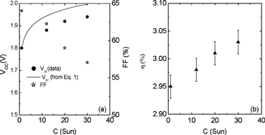
Figure 2: (a) Open-circuit voltage (Voc) and short-circuit current density (Jsc) as functions of solar concentration (C). (b) Solar-energy-to-electricity conversion efficiency ( η) as function of C.
With an incident intensity of 100mW/cm2, the characteristics were: open-circuit voltage 1.8V, closed-circuit current density 2.56mA/cm2, maximum power 2.95mW/cm2. This gives a fill-factor of 64% (2.95/1.8/2.56).
The conversion power efficiency of 2.95% falls short of the ~8% theoretical maximum for the frequency characteristics of the device, but the characteristics are claimed as being ‘significantly higher than previously reported values for InGaN/GaN MQWs solar cells with similar In content in the QWs’. The improvement is attributed to improved InGaN material quality. One of the reasons for the still too low efficiency is the small thickness of the well regions (12x3nm = 36nm). Complete light absorption would require at least 200nm. Evidence for this came from comparing devices with and without a back-reflector. The reflector added 15% to the photocurrent density by effectively doubling the thickness of the well region.
The researchers comment that “obtaining InGaN/GaN MQW structures with a total InGaN light-absorption layer thickness of around 200nm is another challenging task”.
The researchers also studied the device performance under concentrated light conditions of up to 30 suns. The short-circuit current density increases approximately linearly at 2.48mA/cm2/sun. Solar conversion efficiency should improve due to a logarithmic increase in the open-circuit voltage with the number of suns (assuming constant fill-factor). The efficiency increased to 3.03% under 30-sun illumination. The open-circuit voltage increased 8%, falling short of the ~11% expected. This is attributed to a reduction in the fill-factor with increased illumination intensity (57% at 30 suns). The decrease in fill-factor is related to increased recombination at interfaces due to the higher carrier densities at higher levels of illumination.
“However, the results indicate the strong potential of InGaN-based MQW solar cells for concentrated photovoltaic (CPV) applications,” the researchers say.
The group believes that the efficiency under concentrated sunlight could be further enhanced by improving the interfacial quality between InGaN and GaN by reducing the dislocation density at the interface through further growth and device processing optimization.
See related items:
Progress towards high-efficiency InGaN/Si tandem solar cell
![]() Search: InGaN solar cells
Search: InGaN solar cells
Visit: http://link.aip.org
The author Mike Cooke is a freelance technology journalist who has worked in the semiconductor and advanced technology sectors since 1997.
![]() ©2010 Juno Publishing and Media Solutions Ltd. All rights reserved. Semiconductor Today and the editorial material contained within it and related media is the copyright of Juno Publishing and Media Solutions Ltd. Reproduction in whole or part without permission from Juno Publishing and Media Solutions Ltd is forbidden. In most cases, permission will be granted, if the author, magazine and publisher are acknowledged.
©2010 Juno Publishing and Media Solutions Ltd. All rights reserved. Semiconductor Today and the editorial material contained within it and related media is the copyright of Juno Publishing and Media Solutions Ltd. Reproduction in whole or part without permission from Juno Publishing and Media Solutions Ltd is forbidden. In most cases, permission will be granted, if the author, magazine and publisher are acknowledged.
Disclaimer: Material published within Semiconductor Today and related media does not necessarily reflect the views of the publisher or staff. Juno Publishing and Media Solutions Ltd and its staff accept no responsibility for opinions expressed, editorial errors and damage/injury to property or persons as a result of material published.
Semiconductor Today, Juno Publishing and Media Solutions Ltd, Suite no. 133, 20 Winchcombe Street, Cheltenham, GL52 2LY, UK
Web site by No Name No Slogan ![]()