| Home | About Us | Contribute | Bookstore | Advertising | Subscribe for Free NOW! |
| News Archive | Features | Events | Recruitment | Directory |
News
30 August 2010
Improving nitride light emission with silicon dioxide pillars and air gaps
Researchers based at Taiwan’s National Cheng Kung University suggest adding silicon dioxide (SiO2) pillar structures and air gaps as a way to enhance light extraction from nitride light emitting diodes (LEDs) [Wei-Chih Lai et al, Appl. Phys. Lett., vol97, p081103, 2010].
A number of techniques have been developed to enhance light extraction from gallium nitride (GaN) based LEDs, such as laser lift-off, to remove the sapphire substrate, or patterning of the interfaces to enhance transmission out of and reduce internal reflections back into the device.
Embedding air void structures with lower refractive index (1) than GaN (~2.45) has also been reported as a way of increasing light extraction by creating random scattering. The Taiwan researchers used silicon dioxide pillars (refractive index 1.46) and air voids to create a similar random-scattering effect.
Metal-organic chemical vapor deposition was used to grow the nitride epitaxial layers on 2-inch sapphire substrates. The templates consisted of a 30nm GaN nucleation layer grown at 560°C followed by 3μm of undoped GaN grown at 1020°C. A SiO2 layer was then deposited from which the circular pillars (3μm diameter, 3μm spacing) were cut out by inductively coupled plasma etching. The height of the pillar was determined by the thickness of the SiO2 (200nm, 500nm, 700nm). Some of the LEDs tested had no pillars for comparison purposes.
After the pillars were created, the GaN growth was continued using epitaxial layer overgrowth (ELOG) techniques (Figure 1). The air-gaps were created by increasing the lateral growth rate before the silicon pillar was completely covered. This technique created 500nm high air gaps on the 200nm and 500nm pillars. The air gap on the 700nm pillar was 400nm. This smaller gap is attributed to the somewhat different strain conditions in the GaN for the higher pillar changing the lateral overgrowth rates.
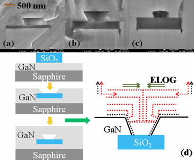
Figure 1: SEM cross-sections of LED with SiO2 pillars and air gap arrays of (a) 200nm and 500nm, (b) 500nm and 500nm, and (c) 700nm and 400nm height SiO2 pillars and air gaps, respectively, and (d) schematic of pillar/air gap formation using ELOG techniques.
Using SiO2 pillars and air gaps should improve not only the light extraction from random scattering, but also the quality of the overlying LED layers. ELOG techniques were developed widely to reduce dislocation densities in nitride material with a view to creating efficient, long lifetime blue laser diodes.
Electronic tests on 250x575 μm LEDs with and without silicon pillars, suggest that the material quality is indeed improved by the ELOG process. For example, the reverse current through the diodes was reduced by more than 50% in the LEDs with pillars (-2.5μA without, -1.3μA with 200nm pillar, -0.9μA with 700nm pillar). The 20mA forward voltage of the LEDs was 3.30V without pillars and 3.34V with 200nm pillars (3.36V with 500nm, 3.38V with 700nm).
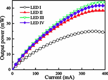 Figure 2: Measured output power vs. injection current for fabricated LEDs. The LEDs are labeled I-IV with increasing pillar height: i.e., I = 0nm (no pillar), II = 200nm, III = 500nm, IV = 700nm.
In terms of electroluminescence, the LED with 500nm pillars had the greatest light output power (Figure 2). All the LEDs emitted around a peak wavelength of 435nm (blue-violet). The measured output power for LEDs with no pillars at 20mA was 3.04mW, while the powers for 200nm, 500nm and 700nm pillar LEDs were 4.23mW (+39.1% on no pillar LED), 4.66mW (+53.3%), and 4.44mW (+46.1%), respectively.
The researchers suggest that the drop in power for the 700nm pillar LED compared with the 500nm one was due to the smaller air gap. The Taiwan group also performed ray-tracing simulations where similar reduction in enhancement with the reduced air gap. Although the simulation showed similar trends in enhancement as for the experimental LEDs, the simulation enhancement values were higher (~70%).
![]() Search: LEDs GaN Sapphire substrates SiO2
Search: LEDs GaN Sapphire substrates SiO2
Visit: http://link.aip.org
The author Mike Cooke is a freelance technology journalist who has worked in the semiconductor and advanced technology sectors since 1997.
![]() ©2010 Juno Publishing and Media Solutions Ltd. All rights reserved. Semiconductor Today and the editorial material contained within it and related media is the copyright of Juno Publishing and Media Solutions Ltd. Reproduction in whole or part without permission from Juno Publishing and Media Solutions Ltd is forbidden. In most cases, permission will be granted, if the author, magazine and publisher are acknowledged.
©2010 Juno Publishing and Media Solutions Ltd. All rights reserved. Semiconductor Today and the editorial material contained within it and related media is the copyright of Juno Publishing and Media Solutions Ltd. Reproduction in whole or part without permission from Juno Publishing and Media Solutions Ltd is forbidden. In most cases, permission will be granted, if the author, magazine and publisher are acknowledged.
Disclaimer: Material published within Semiconductor Today and related media does not necessarily reflect the views of the publisher or staff. Juno Publishing and Media Solutions Ltd and its staff accept no responsibility for opinions expressed, editorial errors and damage/injury to property or persons as a result of material published.
Semiconductor Today, Juno Publishing and Media Solutions Ltd, Suite no. 133, 20 Winchcombe Street, Cheltenham, GL52 2LY, UK
Web site by No Name No Slogan ![]()