| Home | About Us | Contribute | Bookstore | Advertising | Subscribe for Free NOW! |
| News Archive | Features | Events | Recruitment | Directory |
News
8 April 2010
Possible route to better and smaller source/drain contacts for III–V logic
Stanford University researchers have been trying to overcome the limitations of traditional contacts to III-V logic transistors by using single metals with an ultra-thin insulating interlayer rather than alloys [Jenny Hu et al, J. Appl. Phys., vol107, p063712, 2010]. The scientists hope that their work could lead to practical and scalable non-alloyed low-resistance ohmic contacts for III–V metal-oxide-semiconductor field effect (MOSFET) and high-electron-mobility (HEMT) transistors with implanted source/drain contacts, and for tunable barrier heights for III–V Schottky barrier FETs (SB-FETs).
The problem with alloyed contacts is that they can diffuse up to hundreds of nanometers after deposition, creating possible short-circuits. This limits the density at which such contacts can be placed to the order of a micron, far from the desired 20nm or less that is needed to enhance the performance of silicon logic in future commercial devices.
Alloyed contacts are used to create ohmic source/drain contacts for low-resistance current flow into and out of the devices. However, single-metal/III–V contacts tend to have Schottky diode behavior, with low resistance in one direction but a barrier to current flow in the other.
The Schottky barrier needs to be less than 0.1eV for adequate flow of on-current. In the case of III–V materials, the Schottky barrier is increased due to pinning of the Femi energy level and metal-induced gap states (MIGS) at the interface as a result of the more ionic nature of such semiconductors compared with silicon.
Stanford has been applying the idea of putting an ultra-thin layer of insulator between the metal and semiconductor to reduce the Schottky barrier height. This proposal has been applied before to group-IV semiconductors: in silicon in 2004 by intellectual property company Acorn Technologies in Palo Alto, CA, USA and in 2009 at the University of Texas-Dallas, and in the past couple of years on germanium by the University of Tokyo and by Stanford itself. However, the Stanford group believes it is the only one so far to apply these ideas to III–V/metal contacts.
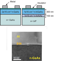 The Stanford work involved metal contacts on lightly doped gallium arsenide and indium gallium arsenide (In0.53Ga0.47As) with ultra-thin interlayers of silicon nitride (SiN) and aluminum oxide (Al2O3) insulator (Figure 1). A variety of metals were tested: yttrium, erbium, aluminum, titanium and tungsten.
Figure 1: Schematic of contact structure (a), and cross-sectional TEM image (b) of Al/SiN/n-GaAs contact, illustrating an amorphous, uniform SiN film.
It is not known exactly why the ultra-thin insulator layer acts to lower the Schottky barrier, rather than just increasing parasitic resistance. By studying the dependence of contact resistance on insulator thickness, the researchers find that SiN is a better candidate for Schottky barrier reduction with Al/GaAs.
Simulations based on a fully self-consistent non-equilibrium Greens function (NEGF) using the effective-mass approximation suggest that increasing the doping from the 2x10¹⁷/cm3 of these experiments to 1x10¹⁹/cm3 would reduce the specific contact resistance from the measured 2.0 Ω-cm2 to a projected 10−7Ω-cm2.
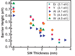 Figure 2: Effective Schottky barrier height extracted from diode measurements between 233K and 353K using thermionic emission model.
Measurements of the effective Schottky barrier height were extracted based on a thermionic emission model for a wide variety of metals and SiN thicknesses (Figure 2), giving values down to ~0.2eV, close to the required values of less than 0.1eV. The researchers believe that further reduction may be possible through use of other dielectric materials.
The researchers also discuss two possible models for the effect of the insulating layer on the Schottky barriers that depends either on changes in metal-induced gap states, or on bond polarizations. On the basis of their work, the Stanford researchers comment: “Currently, the mechanism appears to be from the formation of a positive dielectric dipole, where the ideal dielectric forms a maximum dipole with a minimum band offset to the semiconductor, to achieve the lowest possible contact resistance.”
The Stanford work was supported in part by the Focus Center Research Program, Intel and the US National Science Foundation (NSF).
Visit: http://link.aip.org
The author Mike Cooke is a freelance technology journalist who has worked in the semiconductor and advanced technology sectors since 1997.

![]() ©2010 Juno Publishing and Media Solutions Ltd. All rights reserved. Semiconductor Today and the editorial material contained within it and related media is the copyright of Juno Publishing and Media Solutions Ltd. Reproduction in whole or part without permission from Juno Publishing and Media Solutions Ltd is forbidden. In most cases, permission will be granted, if the author, magazine and publisher are acknowledged.
©2010 Juno Publishing and Media Solutions Ltd. All rights reserved. Semiconductor Today and the editorial material contained within it and related media is the copyright of Juno Publishing and Media Solutions Ltd. Reproduction in whole or part without permission from Juno Publishing and Media Solutions Ltd is forbidden. In most cases, permission will be granted, if the author, magazine and publisher are acknowledged.
Disclaimer: Material published within Semiconductor Today and related media does not necessarily reflect the views of the publisher or staff. Juno Publishing and Media Solutions Ltd and its staff accept no responsibility for opinions expressed, editorial errors and damage/injury to property or persons as a result of material published.
Semiconductor Today, Juno Publishing and Media Solutions Ltd, Suite no. 133, 20 Winchcombe Street, Cheltenham, GL52 2LY, UK
Web site by No Name No Slogan ![]()