| Home | About Us | Contribute | Bookstore | Advertising | Subscribe for Free NOW! |
| News Archive | Features | Events | Recruitment | Directory |
| FREE subscription |
| Subscribe for free to receive each issue of Semiconductor Today magazine and weekly news brief. |
News
29 September 2009
Wafer bonding creates opportunities for Si/GaN integration
Collaboration between Massachussets Institute of Technology (MIT) and Nitronex has resulted in the first on-wafer integration of silicon metal-oxide-semiconductor field-effect transistors (Si MOSFETs) and gallium nitride high-electron-mobility transistors (GaN HEMTs) [Jinwook W. Chung et al, IEEE Electron Device Letters, vol.30, p.1015, October 2009]. The virtual substrate used for the devices consists of a GaN layer sandwiched between two silicon layers. This substrate was created through epitaxy, wafer bonding and etch-back techniques.
The researchers took advantage of the high thermal stability of nitride semiconductors such as GaN to fabricate first the MOSFETs on the top layer and then to etch down to the GaN to produce the HEMTs. This allowed the heterogeneous transistors to be placed less than 5 microns apart.
While silicon is the most versatile material for producing highly dense, high-frequency logic circuits, GaN is attractive for high-frequency power handling in analog/mixed-signal circuits and for its green-to-ultraviolet optoelectronic properties.
A variety of techniques have been used in the past to create such GaN/Si substrates, such as epitaxial growth - including molecular beam epitaxy (MBE), metal-organic chemical vapor deposition (MOCVD) etc - on mis-cut Si(100) and Si(110) substrates. High-quality GaN is difficult to achieve given the large lattice mismatch between the materials and the high density of surface states that arises from the use of mis-cut substrates. Surface states degrade the device performance characteristics.
Nitronex has previously worked on GaN-on-Si integration and has developed an MOCVD process for GaN/Si. The MIT/Nitronex virtual substrate begins (Figure 1) with such MOCVD growth of AlGaN/GaN on a Si(111) wafer, followed by spin-coat deposition of a hydrogen silsesquioxane (HSQ) layer. (Si(111) is not the most suitable material for producing Si MOSFETs.) A silicon-on-insulator (SOI) substrate is then wafer bonded to the HSQ. The Si(111) wafer is removed using a sulfur hexafluoride (SF6) deep reactive ion etch. The structure is then bonded to a Si(100) wafer with another HSQ layer. The 200nm Si(100) top layer is then separated from the SOI handle wafer. A possible simplification of the process would consist of leaving the Si(111) wafer in place and just transferring the Si(100) top layer for the MOSFET devices.
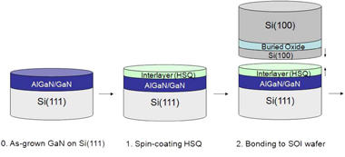
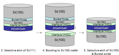
Figure 1: Process for making virtual Si(100)/GaN/Si(100) wafers.
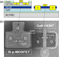
The AlGaN (26% Al) that was used as a barrier layer for the HEMT transistor had a total thickness of 175 Angstroms. At present, the hybrid wafers measure up to 1 inch (25mm) in diameter. The team built p-MOSFETs and used SF6 to etch down to the nitride layers to make the HEMTs.
The gate lengths of the devices are at the micron-scale (1000nm), while state-of-the-art devices produced by Intel and other leading manufacturers are at 45nm and are pushing on towards 32nm. MIT’s Si(100) pMOSFET gate measured about 1.5 microns and the GaN HEMT about 2.5 microns (Figure 2). The devices are reported to have good modulation of the drain current by the gate potential and low off-currents. However, the gate length impacts the maximum output current and MOSFET performance. MIT is working on producing shorter-gate-length MOSFETs.
 The team sees possible applications from such integration as including high-power integrated wireless transmitters, power gating and power conversion circuits, and in-chip optical interconnects based on nitride semiconductor light emitters and silicon digital circuitry.
Figure 2: Schematic and SEM of Si pMOSFETs integrated with GaN HEMTs.
“GaN electronics can be used in a large array of potential applications,” comments professor Tomás Palacios, the leader of the research at MIT. “For example, GaN is very attractive for high-frequency applications due to the very large current densities achievable in these transistors, as well as the large electron velocities. Transistors with a maximum fmax of 300GHz have already been reported and there are programs in place to increase the frequency beyond 500GHz,” he adds. “However, it is true that there are other materials (InGaAs, InSb, etc) are also very promising for these applications.”
“On the other hand, in other applications such as RF power amplifiers and high-voltage power electronics, GaN is clearly the best option and the performance of silicon chips could significantly improve if these devices could be seamlessly combined with silicon CMOS,” says Palacios. “In addition, the integration of GaN and silicon would also allow the fabrication of silicon electronics in close proximity to GaN-based LEDs, lasers and MEMS to enable optical interconnections or energy-harvesting devices.”
Palacios adds that the team is currently developing technology for larger substrates: 4-inch wafers are the first goal (to be ready in the next 2-3 months).
![]() Search: Nitronex GaN HEMTs Wafer bonding
Search: Nitronex GaN HEMTs Wafer bonding
Visit: http://dx.doi.org/10.1109/LED.2009.2027914
The author Mike Cooke is a freelance technology journalist who has worked in the semiconductor and advanced technology sectors since 1997.
![]() ©2009 Juno Publishing and Media Solutions Ltd. All rights reserved. Semiconductor Today and the editorial material contained within it and related media is the copyright of Juno Publishing and Media Solutions Ltd. Reproduction in whole or part without permission from Juno Publishing and Media Solutions Ltd is forbidden. In most cases, permission will be granted, if the author, magazine and publisher are acknowledged.
©2009 Juno Publishing and Media Solutions Ltd. All rights reserved. Semiconductor Today and the editorial material contained within it and related media is the copyright of Juno Publishing and Media Solutions Ltd. Reproduction in whole or part without permission from Juno Publishing and Media Solutions Ltd is forbidden. In most cases, permission will be granted, if the author, magazine and publisher are acknowledged.
Disclaimer: Material published within Semiconductor Today and related media does not necessarily reflect the views of the publisher or staff. Juno Publishing and Media Solutions Ltd and its staff accept no responsibility for opinions expressed, editorial errors and damage/injury to property or persons as a result of material published.
Semiconductor Today, Juno Publishing and Media Solutions Ltd, Suite no. 133, 20 Winchcombe Street, Cheltenham, GL52 2LY, UK
Web site by No Name No Slogan ![]()