| Home | About Us | Contribute | Bookstore | Advertising | Subscribe for Free NOW! |
| News Archive | Features | Events | Recruitment | Directory |
| FREE subscription |
| Subscribe for free to receive each issue of Semiconductor Today magazine and weekly news brief. |
News
12 October 2009
Working towards ZnO/GaN light
A group consisting of three Hong Kong universities (University of Hong Kong, Hong Kong Baptist University, Hong Kong Polytechnic University) and Tawian’s National Tsing Hua University have produced light emitting diodes (LEDs) constructed from zinc oxide (ZnO) nano-rods on a p-type gallium nitride (GaN) epitaxial film [Ng et al, Nanotechnology, vol.20, p.445201, 2009].
With a band gap energy (Eg) of around 3.3eV, in theory ZnO has a similar potential for light emission as GaN (Eg ~ 3.2 - 3.4eV, depending on crystal structure), but at lower cost. However, unlike GaN, suitable p-type doping for ZnO has yet to be worked out.
Given that homojunction ZnO devices are not possible for the time being, many groups have tried to combine n-ZnO with p-type materials such as p-GaN. A number of unusual effects have arisen in these studies, such as light emission under forward and reverse bias, or even under reverse bias only. The spectral composition of the emitted light under these conditions tends to vary depending on the bias. These effects need to be understood if an industrially useful process for producing ZnO-based LEDs is to be developed.
The Hong Kong-Taiwan collaboration aimed to dig into some of these effects using improved light extraction from nano-rod structures, focusing in particular on the impact of different annealing conditions for the magnesium-doped p-GaN epilayer and for the n-ZnO nano-rods.
Four different p-GaN on sapphire substrates were used – two were bought from Epistar in Taiwan, and the remainder grown in-house. The commercial substrates were designed for LED production and included InGaN multi-quantum well layers that complicated the interpretation of the data from the subsequent experiments. One of the in-house substrates was thermally activated by annealing at 825°C in a nitrogen atmosphere, increasing hole carrier concentrations.
The ZnO nano-rods were grown hydrothermally. A seeding step consisted of six cycles of placing droplets of zinc acetate in ethanol solution on the substrate, rinsing and then drying. The seed layer was then annealed at 350°C for 20 minutes. A second seeding step was then carried out in the same way to ensure complete coverage of the substrate.
The nano-rods themselves were produced by putting the seeded substrates in an aqueous solution containing polyethyleneimine, zinc nitrate hydrate and hexamethylene tetramine. The solution was kept at 90°C for 2.5 hours. Then the substrate was put in deionized water and sonicated (subjected to sound energy). Drying was carried out in air at 90°C. Annealing processes were then carried out at 200 or 600°C in either oxygen or argon atmospheres.
To produce devices (Figure 1), a spin-on-glass insulator was applied before the metal contact to prevent unwanted contact between the top contact and exposed areas of the substrate between the rods.
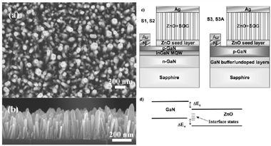
Figure 1: SEM images of nano-rods (a, b), device schematics (c), and sketch of band structure (d).
The commercial substrates exhibited typical backward diode behavior with more current at reverse than forward bias. Backward diode behavior is generally attributed to tunneling currents and is seen when there is a large disparity in carrier concentrations between the n- and p- sides of the diode. The researchers point out that typical carrier concentrations in undoped n-type ZnO are of the order 1018-1019cm-2, while that of Mg-doped p-type GaN is 1017-1018cm-2. The characteristics of the in-house GaN substrate were less pronounced and even almost symmetrical in the forward and reverse bias conditions, in some cases.
Light emission was observed in both directions of bias, although there were large disparities in turn-on voltages (Table 1). The authors suggest that previous work on ZnO nano-rods/GaN LEDs showing emission in only one direction could be explained by the large turn-on voltage needed in one direction (up to 70V). Whether the low turn-on voltage is under forward or reverse bias was found to be determined by the properties of the p-GaN substrate. In fact, only the thermally activated in-house substrate showed more than weak emission under forward bias. A variety of emissions were seen at various bias voltages: ultra-violet, violet, blue, and yellow. The annealed in-house GaN substrate is described as being considerably brighter.
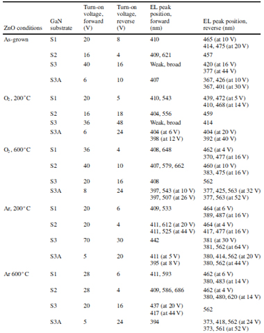
Table 1: Summary of performance of different devices.
The authors conclude that the performance of the light emission is strongly dependent on the energy band alignment between the layers (1.0-2.2eV) and the interface conditions (e.g. whether a mixed region with Ga-O has formed between the GaN and ZnO, which is dependent on anneal temperature).
See related item:
Squeezing light out of silicon
Visit: www.iop.org/EJ
The author Mike Cooke is a freelance technology journalist who has worked in the semiconductor and advanced technology sectors since 1997.
![]() ©2009 Juno Publishing and Media Solutions Ltd. All rights reserved. Semiconductor Today and the editorial material contained within it and related media is the copyright of Juno Publishing and Media Solutions Ltd. Reproduction in whole or part without permission from Juno Publishing and Media Solutions Ltd is forbidden. In most cases, permission will be granted, if the author, magazine and publisher are acknowledged.
©2009 Juno Publishing and Media Solutions Ltd. All rights reserved. Semiconductor Today and the editorial material contained within it and related media is the copyright of Juno Publishing and Media Solutions Ltd. Reproduction in whole or part without permission from Juno Publishing and Media Solutions Ltd is forbidden. In most cases, permission will be granted, if the author, magazine and publisher are acknowledged.
Disclaimer: Material published within Semiconductor Today and related media does not necessarily reflect the views of the publisher or staff. Juno Publishing and Media Solutions Ltd and its staff accept no responsibility for opinions expressed, editorial errors and damage/injury to property or persons as a result of material published.
Semiconductor Today, Juno Publishing and Media Solutions Ltd, Suite no. 133, 20 Winchcombe Street, Cheltenham, GL52 2LY, UK
Web site by No Name No Slogan ![]()