| Home | About Us | Contribute | Bookstore | Advertising | Subscribe for Free NOW! |
| News Archive | Features | Events | Recruitment | Directory |
| FREE subscription |
| Subscribe for free to receive each issue of Semiconductor Today magazine and weekly news brief. |
News
16 October 2009
Fujitsu develops first millimeter-wave GaN transceiver amplifier chipset
At the European Microwave Integrated Circuits Conference (EuMIC) in Rome, Italy (28-29 September), Fujitsu Laboratories Ltd of Kawasaki, Japan announced the development of what is claimed to be the first gallium nitride (GaN) high-electron-mobility transistor (HEMT)-based transceiver amplifier chipset for broadband wireless transmission equipment operating in the millimeter bandwidth (70-100GHz), for which widespread usage is expected to grow.
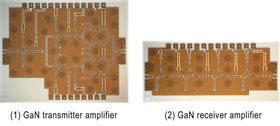 Figure 1: Chipset featuring GaN-based high-output transmitter amplifier and high-sensitivity receiver amplifier.
The new transceiver amplifier chipset (Figure 1) features a GaN HEMT-based transmitter amplifier that achieves what is claimed to be record power output of 350mW plus a high-sensitivity receiver amplifier with record signal gain of 310 operating in the W-band (75-110GHz) with a low noise figure of 3.8dB.
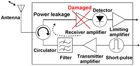 Figure 2: Structure of impulse radio millimeter-wave transceiver.
Compared to gallium arsenide (GaAs)-based technology, power output of the new millimeter-band GaN HEMT-based amplifier chipset is expected to be increased about four-fold (4x) and noise figure reduced by 40%, while transmission ranges are expected to be extended about three-fold (3x). Used as an alternative to fiber-optic cabling, the new transceiver amplifier can help to bridge what Fujitsu calls the digital divide for wireless communications, by making communications equipment for trunk lines and ultra-high-speed fixed wireless access higher in quality and more compact (ultimately making wireless broadband more practical).
To accommodate demands for greater bandwidth on the Internet, cell-phone networks and other networks, fiber-optic cabling is being laid throughout Japan to create a high-capacity trunk-line system. However, this is problematic in heavily built-up areas, or areas with difficult topography, which has sparked interest in high-bandwidth wireless that is capable of data transmission capacities and speeds of 10Gb/s - on a par with fiber-optic cabling - as a way to bridge the digital divide.
The millimeter-wave band (70-100GHz) can be an effective band for wireless communications running faster than 10Gb/s, as it is readily available and appropriate for long-distances transmissions. Fujitsu Laboratories has tested millimeter-band transmitters and receivers at speeds of 10Gb/s using impulse radio (which emits a broadband pulse signal that varies over a very short period, and uses a filter to extract only the usable frequency component for transmission). However, for this to be practical and widely used, transmission distances would need to be extended from several kilometers to several tens of kilometers.
One way to achieve this would be through higher-output amplifiers. But higher outputs cause increased power leakage from the transmitter to the receiver, which can overload the inputs of circuits using existing technologies based on gallium arsenide and indium phosphide (InP), resulting in breakdown. There has hence been a desire to develop GaN-based receiver amplifiers, as they can tolerate higher inputs and have excellent reception sensitivity.
To satisfy the above requirements for W-band signals, the transceiver amplifier needs to address the following issues:
- Compared to conventional GaAs HEMT devices, the wide-bandgap characteristics of GaN HEMT devices enable breakdown voltages that are ten times greater (10x), allowing them to tolerate higher voltages. However, because the parasitic capacitance of transistors worsens with high-frequency signals of 70GHz or higher, the signal amplification rate to magnify weak incoming signals - to enable them to be identified - is insufficient, as the incoming signals become buried in noise.
- At frequencies above 70GHz, the signal wavelength is roughly the same length as the chip size, which produces signal interference that is more prominent, between signal paths and circuits. This makes it difficult to create an integrated circuit featuring good signal amplification and low noise, due to the fact that oscillation of the circuit itself can result in malfunctions caused by unnecessary power-coupling between the signal paths.
Fujitsu says that it has addressed the above issues through the following technologies:
- In 2006, Fujitsu Laboratories developed a GaN HEMT structure with gate lengths of just 0.12 microns, allowing for both high breakdown voltage and good high-frequency performance. By tuning this gate structure and adjusting the thickness of the protective layer, parasitic capacitance was reduced, and the increased signal gain further improved noise characteristics (Figure 3).
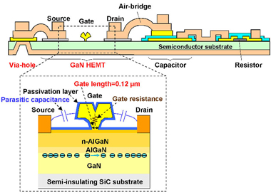
Figure 3: Cross section of high breakdown-voltage millimeter-wave GaN HEMT.
- As the output of GaN HEMTs is higher than existing devices, signal interference (caused by unnecessary signal emissions from signal circuitry) between signal paths and circuits is more prominent in GaN HEMTs. By laying contact conductors around the signal circuitry while employing a 3D electromagnetic field analysis to optimize the placement of via-holes that penetrate the top and bottom of the chip relative to signal paths and circuits, and by developing design technology that shields against unnecessary signal radiation - and applying all of these for the first time in GaN HEMT circuitry - signal interference has been suppressed (Figure 4). These millimeter-wave circuit stabilization technologies realize a circuit that features high output and high signal-gain while being able to operate stably, free from malfunctions caused by circuit oscillations.
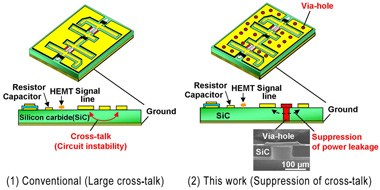
Figure 4: New stabilization technology for millimeter-wave circuits.
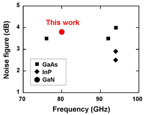 Figure 5: Comparison of millimeter-wave receiver amplifier performance (first report for GaN-based).
The new receiver-amplifier operates in the W-band with a signal gain rate of 25dB (310x) and a noise figure of 3.8dB - both records for a GaN-based IC (Figure 5). Fujitsu says that the amplifier unit's receiver performance is on a par with those using GaAs-based technology but, because it obviates the need for a protective circuit, the performance of the transceiver as a whole can be expected to improve (Figure 6).
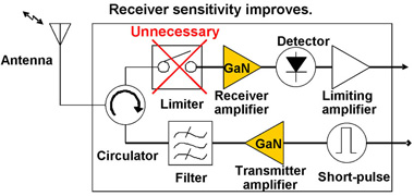
Figure 6: Structure of impulse radio millimeter-wave transceiver.
Fujitsu says that it aims to continue improving the performance and expanding the frequency band for GaN circuits featuring high breakdown-voltages, in order to enable wireless equipment that can be used as an alternative to fiber-optic networks.
See related items:
Fujitsu develops GaN HEMT for use in power supplies
Fujitsu claims first 100W X-band high-output amplifier with efficiency over 50%
![]() Search: Fujitsu Laboratories GaN HEMTs
Search: Fujitsu Laboratories GaN HEMTs
Visit: http://jp.fujitsu.com/group/labs/en
![]() ©2009 Juno Publishing and Media Solutions Ltd. All rights reserved. Semiconductor Today and the editorial material contained within it and related media is the copyright of Juno Publishing and Media Solutions Ltd. Reproduction in whole or part without permission from Juno Publishing and Media Solutions Ltd is forbidden. In most cases, permission will be granted, if the author, magazine and publisher are acknowledged.
©2009 Juno Publishing and Media Solutions Ltd. All rights reserved. Semiconductor Today and the editorial material contained within it and related media is the copyright of Juno Publishing and Media Solutions Ltd. Reproduction in whole or part without permission from Juno Publishing and Media Solutions Ltd is forbidden. In most cases, permission will be granted, if the author, magazine and publisher are acknowledged.
Disclaimer: Material published within Semiconductor Today and related media does not necessarily reflect the views of the publisher or staff. Juno Publishing and Media Solutions Ltd and its staff accept no responsibility for opinions expressed, editorial errors and damage/injury to property or persons as a result of material published.
Semiconductor Today, Juno Publishing and Media Solutions Ltd, Suite no. 133, 20 Winchcombe Street, Cheltenham, GL52 2LY, UK
Web site by No Name No Slogan ![]()