| Home | About Us | Contribute | Bookstore | Advertising | Subscribe for Free NOW! |
| News Archive | Features | Events | Recruitment | Directory |
| FREE subscription |
| Subscribe for free to receive each issue of Semiconductor Today magazine and weekly news brief. |
News
6 November 2009
Sharp’s AlInN route to inner-stripe blue-violet laser power
Researchers at Sharp Corp’s Advanced Technology Research Laboratories in Japan and Sharp Laboratories of Europe Ltd in the UK have used lattice-matched aluminum indium nitride (AlInN) to improve blue-violet laser output power [Wei-Sin Tan et al, Appl. Phys. Express, vol2, p112101, 2009]. The AlInN material is used as a current-confinement layer for inner-stripe laser diodes (Figure 1).
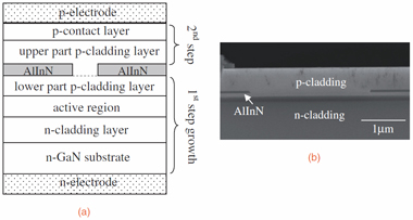
Figure 1: Sharp’s inner-stripe laser diode structure (a) and cross-sectional SEM of grown device (b).
The researchers are targeting emission wavelengths of around 405nm, as used for high-density optical storage such as Blu-ray and high-definition DVD (HD-DVD). Higher-power laser diodes would be advantageous for optical storage, as they give the possibility for increased data transfer rates. The researchers also see opportunities for high-brightness light sources and laser projector systems.
Presently, lasers constructed using ridge structures have low wall-plug efficiency (WPE), resulting in heat generation at high operating powers. Heat degrades laser operation and can ultimately lead to catastrophic failure.
By using an inner stripe, one can mitigate the poor conductivity of top p-type aluminum gallium nitride (p-AlGaN) cladding and p-type gallium nitride (p-GaN) contact layers by allowing the current to flow across a wider area. It is these layers that in a narrow ridge structure have high resistance and hence generate heat under high voltages.
Some previous work with inner stripe laser diodes has used aluminum nitride (AlN) as the current-blocking layer. Sharp used undoped lattice-matched AlInN (with an indium composition of 17%), since this should reduce strain build-up and hence tendencies towards cracking and defects. These factors would be expected to improve the quality of subsequent layers.
Sharp’s devices were grown on n-type (0001)-face GaN substrates from Japan’s Sumitomo Electric Industries Ltd. The initial layers to the lower part of the p-type cladding were grown using metal-organic chemical vapor deposition (MOCVD). These were: n-Al0.06Ga0.94N cladding, n-GaN waveguide, a triple InGaN quantum-well active region, p-Al0.30Ga0.70N to prevent evaporation, and the lower p-Al0.06Ga0.94N cladding.
Plasma-assisted molecular beam epitaxy (MBE) was then used to deposited a 50nm layer of Al0.83In0.17N. The laser stripe aperture (with a width of 2-6μm) was then created using lift-off techniques with a silicon dioxide sacrificial layer. The MBE process creates resistive AlInN material (10 3Ω-cm), rather than the usual n-type material that results from undoped AlInN grown using MOCVD. The usual n-type characteristic of AlInN has been attributed to nitrogen vacancies or oxygen impurities. The Sharp group sees further application potential for their resistive MBE-grown AlInN.
The wafer was then returned to MOCVD layer growth of the upper cladding, ensuring optimal conditions for a smooth interface between the upper and lower parts of the cladding.
The p- and n- metal contacts consisted of palladium/gold (Pd/Au) and titanium/aluminum/gold (Ti/Al/Au), respectively.
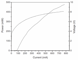 Typical uncoated devices achieved continuous-wave (CW) lasing at a threshold current density of 3.3-3.5kA/cm2 and a slope efficiency of 0.8-0.9W/A. The researchers comment that these values are comparable to those of ridge laser diodes. A 4.3x600μm2 device achieved a peak slope efficiency of 1.6W/A and could be operated at up to 800mA under a 0.1% duty cycle of pulsed power (Figure 2).
Figure 2: Pulsed output power-current-voltage (L-I-V) plot for 4.3x600μm2 device (p-side up) at 25°C.
Kinks in the optical power-current (L-I) plot are attributed to multi-mode laser generation effects, which could be eliminated by using narrower stripes of 1.0-1.5μm width.
Reliability tests were carried out for a 2.8μm-width device operated under CW conditions at 25°C. The current was increased over time to maintain a constant output power of 50mW. Extrapolating from the 400 hour operation, the researchers give a lifetime (to 1.3x the initial operating current) of 1000 hours. The researchers note that scanning electron microscope (SEM) investigations showed no obvious damage to the re-growth interface resulting from the testing.
Simulations suggest that reducing the stripe width could give further benefits over equivalent ridge structures. The researchers are hence working towards achieving these benefits experimentally, particularly in terms of lower operating voltages and reduced thermal roll-over effects.
While Sharp does not supply components commercially, Nichia laser diode engineering samples are listed at up to 500mW output power, and up to 200mW for marketed products.
![]() Search: Sharp AlInN Blue-violet laser MBE
Search: Sharp AlInN Blue-violet laser MBE
Visit: http://apex.ipap.jp/link?APEX/2/112101/
Visit: http://sharp-world.com/products/index.html
Visit: www.nichia.com/product/laser-main.htmlThe author Mike Cooke is a freelance technology journalist who has worked in the semiconductor and advanced technology sectors since 1997.
![]() ©2009 Juno Publishing and Media Solutions Ltd. All rights reserved. Semiconductor Today and the editorial material contained within it and related media is the copyright of Juno Publishing and Media Solutions Ltd. Reproduction in whole or part without permission from Juno Publishing and Media Solutions Ltd is forbidden. In most cases, permission will be granted, if the author, magazine and publisher are acknowledged.
©2009 Juno Publishing and Media Solutions Ltd. All rights reserved. Semiconductor Today and the editorial material contained within it and related media is the copyright of Juno Publishing and Media Solutions Ltd. Reproduction in whole or part without permission from Juno Publishing and Media Solutions Ltd is forbidden. In most cases, permission will be granted, if the author, magazine and publisher are acknowledged.
Disclaimer: Material published within Semiconductor Today and related media does not necessarily reflect the views of the publisher or staff. Juno Publishing and Media Solutions Ltd and its staff accept no responsibility for opinions expressed, editorial errors and damage/injury to property or persons as a result of material published.
Semiconductor Today, Juno Publishing and Media Solutions Ltd, Suite no. 133, 20 Winchcombe Street, Cheltenham, GL52 2LY, UK
Web site by No Name No Slogan ![]()