| Home | About Us | Contribute | Bookstore | Advertising | Subscribe for Free NOW! |
| News Archive | Features | Events | Recruitment | Directory |
| FREE subscription |
| Subscribe for free to receive each issue of Semiconductor Today magazine and weekly news brief. |
News
20 November 2009
Pit-stop towards improved AlGaN-on-Si HEMT breakdown
Deep pits that arise in growth of aluminum gallium nitride (AlGaN) high-frequency power transistors on silicon substrates give rise to increased leakage and lower breakdown voltages, according to research at the Nagoya Institute of Technology in Japan [Selvaraj, Appl. Phys. Express, vol2, p111005, 2009].
During the past few years AlGaN semiconductor material has been developed beyond its original light-emitting applications into the high-frequency power transistor market (up to ~30GHz). Potential applications include power amplification for the transmission of radio and microwave signals, such as for mobile phone network connections to the main telephone network.
To enable high breakdown voltages, as required for these applications, material quality is a vital concern. However, there is also the concern of competing with other technologies based in lower-cost production processes using silicon or gallium arsenide. A recent development with cost-cutting potential is the growth of gallium nitride (GaN) on silicon rather than the much more expensive silicon carbide. The other common substrate for GaN — sapphire — is often not suitable for power applications because of its poor thermal conductivity.
Silicon-based GaN also has scale-up potential to larger wafers (up to 300mm diameter), creating economies of scale. The penalty for growing GaN on Si is that the large lattice mismatch (~17%) between the materials negatively impacts material quality.
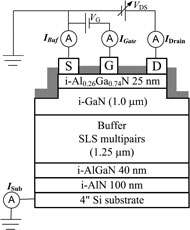 The Nagoya researchers used Taiyo Nippon Sanso’s SR4000 horizontal metal-organic chemical vapor deposition (MOCVD) system to grow AlGaN/GaN high-electron-mobility transistors (HEMTs) on 4-inch silicon substrates (Figure 1). The buffer layers used to transition between the silicon and the GaN lattices included layers of AlN, AlGaN and a super-lattice structure.
Figure 1: AlGaN HEMT structure used to investigate impact of deep pits on breakdown performance (SLS = super-lattice structure).
A variety of pit structures and densities were found for different wafers, even with the same buffer scheme and total epilayer thickness. In particular, there were two types of pit: shallow ones (that require atomic force microscopic detection) and deep ones (that need only an ordinary microscope to be observed). The deep pits have hexagonal pyramid structures.
The aim of the research was to investigate the three-terminal-off breakdown characteristics of the HEMTs. When the transistor is nominally ‘off’ (i.e. the gate is below threshold), a variety of leakage currents can occur through the gate, buffer and substrate. The combination of these leakage currents is reflected in the drain leakage current.
The researchers tested their HEMTs with a constant -5V gate bias, which is well below the threshold for the transistor. The breakdown behavior of the devices depended on the deep pit density of the substrate, but not on the shallow pits.
A device with almost no deep pits had a breakdown of about 325V, although the gate leakage is rather high due to the use of a Schottky barrier, rather than an insulator/oxide structure. At an intermediate deep pit density of 2:5x10³/cm2, buffer and substrate leakage increase to be of similar size to that through the gate, and breakdown occurs at 246V. A further increase in density (3x10⁴/cm2) reduces the breakdown to 130V, due to a leap in substrate leakage. The maximum pit density substrate used (7.5x10⁵/cm2) yielded devices with breakdowns of only 48V.
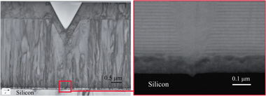
Figure 2: TEM across deep pit on GaN surface originating from Si substrate (left). SEM of etch pit at the AlN/Si junction.
The researchers used transmission (TEM) and scanning (SEM) electron microscopy to investigate the source of the deep pits on GaN substrates having a thicker 4μm buffer. The resulting images suggest that the deep pits originate from the surface of the silicon substrate (Figure 2, left). Looking more closely at the origin of the pit, one finds a pit in the silicon surface itself (Figure 2, right). The disruption in growth caused by these pits means that deep surface pits arise irrespective of the thickness of the subsequent buffer layers. The pits in the silicon surface can arise from the etching effect of Ga in the MOCVD process. The researchers found etching to occur even when an AlN layer was used to prevent such action by Ga.
The researchers conclude that deep pits found on the surface originate from the silicon substrate and behave like micro-pipes for high substrate current leakage. The deep pits not only affect the buffer and substrate leakage but also boost gate leakage. The researchers believe that this is due to a high density of tunneling paths from defect levels caused by poor crystal quality and a lowering of the Schottky barrier as a result of higher free-carrier densities.
![]() Search: AlGaN-on-Si HEMT
Search: AlGaN-on-Si HEMT
Visit: http://apex.ipap.jp/link?APEX/2/111005
Visit: http://eng.nitech.ac.jp
The author Mike Cooke is a freelance technology journalist who has worked in the semiconductor and advanced technology sectors since 1997.
![]() ©2009 Juno Publishing and Media Solutions Ltd. All rights reserved. Semiconductor Today and the editorial material contained within it and related media is the copyright of Juno Publishing and Media Solutions Ltd. Reproduction in whole or part without permission from Juno Publishing and Media Solutions Ltd is forbidden. In most cases, permission will be granted, if the author, magazine and publisher are acknowledged.
©2009 Juno Publishing and Media Solutions Ltd. All rights reserved. Semiconductor Today and the editorial material contained within it and related media is the copyright of Juno Publishing and Media Solutions Ltd. Reproduction in whole or part without permission from Juno Publishing and Media Solutions Ltd is forbidden. In most cases, permission will be granted, if the author, magazine and publisher are acknowledged.
Disclaimer: Material published within Semiconductor Today and related media does not necessarily reflect the views of the publisher or staff. Juno Publishing and Media Solutions Ltd and its staff accept no responsibility for opinions expressed, editorial errors and damage/injury to property or persons as a result of material published.
Semiconductor Today, Juno Publishing and Media Solutions Ltd, Suite no. 133, 20 Winchcombe Street, Cheltenham, GL52 2LY, UK
Web site by No Name No Slogan ![]()