| Home | About Us | Contribute | Bookstore | Advertising | Subscribe for Free NOW! |
| News Archive | Features | Events | Recruitment | Directory |
| FREE subscription |
| Subscribe for free to receive each issue of Semiconductor Today magazine and weekly news brief. |
News
7 May 2009
X-ray reveals anatomy of gallium oxide
University of Texas at Dallas (UT Dallas) researchers have been using x-ray photoelectron spectroscopy (XPS) to determine the impact of oxides on gallium arsenide (GaAs) and indium gallium arsenide (InGaAs) surfaces for electronic applications [Hinkle et al, App. Phys. Lett., vol.94, p.162101, 2009]. Such studies are important if metal-oxide-semiconductor field-effect transistor (MOSFET) devices based on higher-mobility InGaAs channels are to become available to extend complementary MOS (CMOS) electronics during the next decade. CMOS is the standard device configuration used in digital electronics. A GaAs MOSFET could also be a useful addition to III-V electronics capabilities.
Existing CMOS electronics based on silicon has benefited from the ease with which a good interface can be made between the silicon MOSFET channel and the silicon dioxide gate insulator. In particular, one needs to avoid interface charge traps that can alter the device’s behavior with use. Charges at the interface can pin the Fermi energy level in the channel. In such a situation, the gate no longer has the ability to adequately control the channel current.
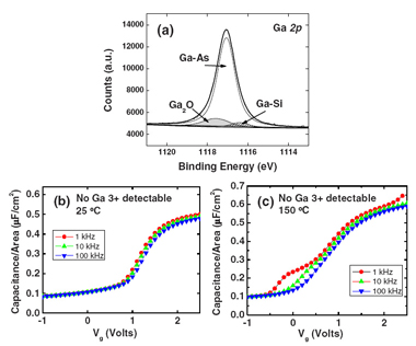
The UT Dallas researchers find that the presence of stable Ga2O states at the interface is not detrimental to the performance of GaAs/InGaAs devices. However, removing the Ga 3+ oxidation state (Ga2O3) results in a reduction in frequency dispersion in capacitor-voltage (C-V) measurements. Low dispersion indicates fewer trap states.
XPS uses the photoelectric effect, where monochromatic x-rays eject electrons from the surface of a material. Peaks in the electron energy spectrum can be associated with particular initial energy states near the surface of the material. These initial energies are dependent on the bonding configuration of the atoms.
Studies using XPS normally concentrate on changes in the outer 3d electron states in Ga with particular bonding configurations. These studies are usually performed at large synchrotron light source facilities with high photon intensities. Laboratory-level XPS can be performed with aluminum Kα x-ray sources, resulting in photoelectrons with 3d energies of ~1465eV, but the sensitivity to surface electrons is low. Higher surface sensitivity (~3nm) can be obtained from studying the more tightly bound 2p spectrum with photoelectron energies of ~369eV, but the peak shifts are smaller and the peak profiles are broader. These factors make the separation of the peaks and their assignment to various bond configurations quite delicate.
With Ga2O3 (3+)
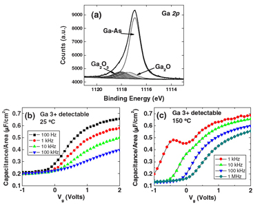
Graphics: Results of XPS analysis (top of respective figures) and CV measurements at 25ºC and 150ºC showing the impact of the presence of Ga2O3 (Ga 3+ state) at the GaAs surface. The dielectric in both cases is 1nm of Al2O3 deposited with atomic layer technology (ALD). The surface without Ga2O3 had a extra layer of 1.2nm ex-situ plasma-enhanced chemical vapor deposited amorphous silicon that was applied before the Al2O3.
Without Ga2O3 (3+)
Despite the difficulties, the researchers performed measurements on the 2p spectrum in-situ, i.e. in the environment used to grow the surface layers. The in-situ measurement adds extreme control by allowing the growth of surfaces with precise compositions and avoiding exposure to spurious contaminants such as carbon, oxygen and water.
“We produced an atomically clean surface and interrogated the surface by XPS to measure the ‘clean’ Ga peak position and shape, which is therefore indicative of only Ga-As bonding and therefore serves as a ‘control sample’ spectrum," explains professor Robert M Wallace, leader of the UT Dallas group. "We then examined this same surface after in-situ thin-film deposition or even ex-situ chemical treatments to look at how the peak position or shape changes.”
The group claims to have conclusively identified three oxidation states and a Ga-Si bond. The latter bond is of interest because silicon passivation is used to improve the performance of III-V MOS devices. The states were determined using carefully controlled surfaces to find the XPS peaks for GaAs bulk material, Ga2O (Ga 1+ oxidation state), Ga2O3 (Ga 3+) and Ga-Si. The Ga2+ state (GaO) was not detected in the samples.
“Without the in-situ capability, the careful deconvolution of the Ga 1+ state would not be possible with a high degree of confidence," comments Wallace. "Since we can, for example, purposely deposit a Ga2O layer in-situ, we can detect the broadening of the Ga 2p feature from the original atomically clean state, and therefore confidently deconvolve the spectral feature into the constituent peaks," he adds. "We then test this interpretation with a variety of other surface treatments and fitting procedures to check for self-consistency. We have also looked at thin ALD growth using this approach.”
![]() Search: GaAs InGaAs MOSFET CMOS
Search: GaAs InGaAs MOSFET CMOS
Visit: http://link.aip.org
Visit: www.utdallas.edu
The author Mike Cooke is a freelance technology journalist who has worked in the semiconductor and advanced technology sectors since 1997.

![]() ©2009 Juno Publishing and Media Solutions Ltd. All rights reserved. Semiconductor Today and the editorial material contained within it and related media is the copyright of Juno Publishing and Media Solutions Ltd. Reproduction in whole or part without permission from Juno Publishing and Media Solutions Ltd is forbidden. In most cases, permission will be granted, if the author, magazine and publisher are acknowledged.
©2009 Juno Publishing and Media Solutions Ltd. All rights reserved. Semiconductor Today and the editorial material contained within it and related media is the copyright of Juno Publishing and Media Solutions Ltd. Reproduction in whole or part without permission from Juno Publishing and Media Solutions Ltd is forbidden. In most cases, permission will be granted, if the author, magazine and publisher are acknowledged.
Disclaimer: Material published within Semiconductor Today and related media does not necessarily reflect the views of the publisher or staff. Juno Publishing and Media Solutions Ltd and its staff accept no responsibility for opinions expressed, editorial errors and damage/injury to property or persons as a result of material published.
Semiconductor Today, Juno Publishing and Media Solutions Ltd, Suite no. 133, 20 Winchcombe Street, Cheltenham, GL52 2LY, UK
Web site by No Name No Slogan ![]()