| Home | About Us | Contribute | Bookstore | Advertising | Subscribe for Free NOW! |
| News Archive | Features | Events | Recruitment | Directory |
| FREE subscription |
| Subscribe for free to receive each issue of Semiconductor Today magazine and weekly news brief. |
News
5 May 2009
Light-enhanced wet etch eats into GaN
Researchers at the University of Crete and the Greek Foundation for Research and Technology Institute of Electronic Structure & Laser (FORTH/IESL) are developing wet etch techniques for use with nitride-based semiconductors [Trichas et al, App. Phys. Lett, vol.94, p.173505, 2009]. Illumination with ultraviolet light is used to enable the etch process. Further, by using light with a well defined wavelength, they are able to selectively etch into some III-nitride materials and not others.
Normally, group III-nitrides such as GaN are highly resistant to wet chemical etching methods, so plasma techniques have to be used. However, plasma processing tends to leave ion-induced damage and rough sidewalls in its wake. For optoelectronic devices, such as lasers, smooth sidewalls for cavities can be extremely important.
 The researchers use a tuned titanium-doped sapphire laser to produce narrow-spectrum illumination to create a resonantly enhanced selective photochemical etch process.
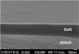
Picture: SEM photo of GaN on AlGaN etch.
The electrochemical solution is potassium hydroxide (KOH) in water. The anode is formed by the GaN film surface, while the cathode is made of platinum. A 100nm-thick titanium layer patterned with square holes was used as the etch mask.
The Ti:sapphire laser produced 150 femtosecond pulses with a wavelength tuning range of 670-760nm. The nonlinear photonic crystal beta barium borate (BBO) was used to double the frequency of the radiation (3.3-3.6eV) to the range of GaN’s bandgap (~3.4eV).
The researchers measured the photocurrent at various excitation energies and found a resonance around 3.43eV associated with exciton absorption. The exciton enhancement has not been seen before by other groups exploring photochemical etching. The Crete scientists believe that this is due to the excitation sources in these other experiments being more broadband.
The wet etch process actually occurs under a reverse bias that confines holes to the GaN surface, where they enable the oxidation of the Ga from the GaN film.
Scanning electron microscope (SEM) characterization of the etch results for various frequencies of excitation followed cleaning with a strong KOH solution to remove oxide by-products. The greatest etch depth of 2 microns occurred at 3.43eV, while at 3.36eV there was a small amount of roughening of the surface and at 3.54eV the etch process reached down only 650nm.
The researchers investigated the same process with an Al0.32Ga0.68N film with a wider bandgap and found no etching at all at 3.43eV. This selectivity opens up the hope that the process could be useful for processing nitride semiconductors, particularly those requiring optical flatness.
A final experiment looked at structures that combined layers of pure GaN with AlGaN. In particular, GaN was deposited on a 100nm layer of Al0.2Ga0.8N. The wet etch with ~3.4eV illumination consumed the GaN layer but stopped when it reached the AlGaN (Figure). Again, a Ti patterned mask was used.
The researchers in Crete have been developing the photochemical etch for a while. Last year, they studied the etch technique on separate samples of GaN and AlGaN [Trichas et al, phys. stat. sol. (a) vol.205, p.2509, 2008].
Visit: http://link.aip.org/link/?APPLAB/94/173505/1
Visit: http://dx.doi.org/10.1002/pssa.200780215
Visit: www.materials.uoc.gr/~psav
Visit: www.iesl.forth.gr/index.aspx
The author Mike Cooke is a freelance technology journalist who has worked in the semiconductor and advanced technology sectors since 1997.

![]() ©2009 Juno Publishing and Media Solutions Ltd. All rights reserved. Semiconductor Today and the editorial material contained within it and related media is the copyright of Juno Publishing and Media Solutions Ltd. Reproduction in whole or part without permission from Juno Publishing and Media Solutions Ltd is forbidden. In most cases, permission will be granted, if the author, magazine and publisher are acknowledged.
©2009 Juno Publishing and Media Solutions Ltd. All rights reserved. Semiconductor Today and the editorial material contained within it and related media is the copyright of Juno Publishing and Media Solutions Ltd. Reproduction in whole or part without permission from Juno Publishing and Media Solutions Ltd is forbidden. In most cases, permission will be granted, if the author, magazine and publisher are acknowledged.
Disclaimer: Material published within Semiconductor Today and related media does not necessarily reflect the views of the publisher or staff. Juno Publishing and Media Solutions Ltd and its staff accept no responsibility for opinions expressed, editorial errors and damage/injury to property or persons as a result of material published.
Semiconductor Today, Juno Publishing and Media Solutions Ltd, Suite no. 133, 20 Winchcombe Street, Cheltenham, GL52 2LY, UK
Web site by No Name No Slogan ![]()