| Home | About Us | Contribute | Bookstore | Advertising | Subscribe for Free NOW! |
| News Archive | Features | Events | Recruitment | Directory |
| FREE subscription |
| Subscribe for free to receive each issue of Semiconductor Today magazine and weekly news brief. |
News
24 June 2009
Fujitsu develops GaN HEMT for use in power supplies
At this week’s Device Research Conference (DRC 2009) at Penn State University, Fujitsu Laboratories Ltd of Kawasaki, Japan presented the development of a new structure for gallium nitride high-electron-mobility transistors (GaN HEMTs) that is claimed to be able to minimize power loss in power supplies, enabling reduced power consumption by electronic equipment such as IT hardware and home electronics.
For power supplies used in electronic hardware (Figure 1), power lost as heat can account for 30% or more of the total power consumed by the device. Also, waste heat creates the need for additional cooling equipment, resulting in a ripple effect of increased power consumption, says Fujitsu.
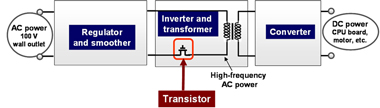
Figure 1: Schematic view of power supply.
A desirable characteristic for power supplies used in products such as PCs, home appliances and automobiles is therefore complete current interruption in standby mode, in which no voltage is applied to the gate electrodes. Conventional GaN HEMTs have required a negative gate voltage to be applied when in standby.
In 2008, Fujitsu Laboratories developed a three-layer cap structure for GaN HEMTs - by sandwiching an aluminium nitride (AlN) layer between n-type GaN layers - which can suppress the current when in standby (Figure 2). The new GaN HEMT structure was originally developed for wireless transmission amplifiers. However, because the voltage that was applied at the gate electrode in order to switch between on and off states (the turn-on voltage) was in the range of 0.5V, it could not be used for power supplies, which need to apply +2-4V in order to apply hundreds of volts at the drain electrode. In addition, power supplies effectively need to have an on-state current density of at least 600mA/mm.
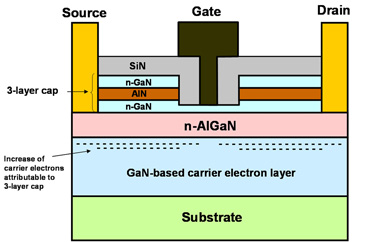
Figure 2: GaN HEMT structure developed by Fujitsu in 2008 for wireless communication base-station amplifiers.
In addition to the three-layer cap structure, Fujitsu made the two following GaN HEMT advances (see Figure 3):
- A technology was developed for precise removal of the cap layers and part of the AlGaN layer only beneath the gate electrode. By leaving a thin n-type AlGaN layer on the GaN carrier layer, while suppressing damage to the GaN layer, on-state voltage can be increased beyond +2V while preserving the total interruption in standby, enabling high-speed performance when turned on.
- A gate structure was developed that uses an insulated-gate structure with an atomic-layer-controlled oxide film that has atom-level flatness. Because this suppresses gate leakage current in which travelling electrons flow to the gate electrode when turned on, a positive voltage can be applied to the gate electrode, resulting in high on-state current density.
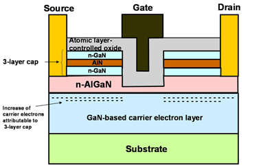
Figure 3: Fujitsu’s new GaN HEMT structure for power supplies.
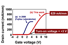 The on-state voltage of the new transistor reaches +3V, which can easily be applied to power supplies while achieving a current density of 829mA/mm - double that of the transistor design on which it is based - resulting in high current values (Figure 4).
Figure 4: Transistor characteristics of the new GaN HEMT.
Among transistors that can achieve an on-state voltage of at least +2V and completely interrupt current when off, the new transistor features record on-state current density, making it the first GaN HEMT that has the characteristics required for power supply, it is claimed (Figure 5).
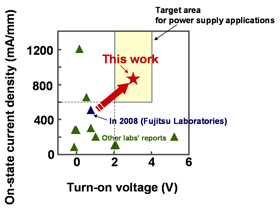 Figure 5 (right): Maximum current density and turn-on voltage (threshold voltage) benchmarks for the new GaN HEMT (transistors with a breakdown voltage of 100V or higher in which current can be interrupted during standby without applying a negative gate voltage).
Since the new GaN HEMT technology blocks the flow of current from power supplies in standby mode and produces high on-state current density, it has the potential to cut power consumption of electronic equipment by one-third, compared to that of power supplies based on conventional silicon transistors, Fujitsu reckons. Extrapolated to all data centers in Japan - and taking into account the knock-on benefits of energy savings enabled through reduced air-conditioning electricity required for cooling - this could cut data-center power consumption in Japan by 12%, cutting the country’s total CO2 emissions by 330,000 tons, it is reckoned.
Also, the high-frequency performance of the new transistors can enable more compact power supplies. High-speed transistor operation would allow for more compact coils and transformers, which have been particularly difficult to miniaturize in conventional power supplies with low-frequency operation: the size of AC adapters for notebook PCs, for example, could be reduced to one-tenth of current sizes, says Fujitsu. Smaller power supplies would also contribute to reducing space requirements for data centers.
Fujitsu says that it is progressing with practical implementations of GaN transistors featuring high breakdown voltages, with the aim of producing power supplies based on them by about 2011.
See related item:
Fujitsu claims first 100W X-band high-output amplifier with efficiency over 50%
![]() Search: Fujitsu Laboratories GaN HEMTs
Search: Fujitsu Laboratories GaN HEMTs
Visit: http://jp.fujitsu.com/group/labs/en
![]() ©2009 Juno Publishing and Media Solutions Ltd. All rights reserved. Semiconductor Today and the editorial material contained within it and related media is the copyright of Juno Publishing and Media Solutions Ltd. Reproduction in whole or part without permission from Juno Publishing and Media Solutions Ltd is forbidden. In most cases, permission will be granted, if the author, magazine and publisher are acknowledged.
©2009 Juno Publishing and Media Solutions Ltd. All rights reserved. Semiconductor Today and the editorial material contained within it and related media is the copyright of Juno Publishing and Media Solutions Ltd. Reproduction in whole or part without permission from Juno Publishing and Media Solutions Ltd is forbidden. In most cases, permission will be granted, if the author, magazine and publisher are acknowledged.
Disclaimer: Material published within Semiconductor Today and related media does not necessarily reflect the views of the publisher or staff. Juno Publishing and Media Solutions Ltd and its staff accept no responsibility for opinions expressed, editorial errors and damage/injury to property or persons as a result of material published.
Semiconductor Today, Juno Publishing and Media Solutions Ltd, Suite no. 133, 20 Winchcombe Street, Cheltenham, GL52 2LY, UK
Web site by No Name No Slogan ![]()