| Home | About Us | Contribute | Bookstore | Advertising | Subscribe for Free NOW! |
| News Archive | Features | Events | Recruitment | Directory |
| FREE subscription |
| Subscribe for free to receive each issue of Semiconductor Today magazine and weekly news brief. |
News
31 July 2009
Buffer boost for InGaN on silicon solar cell
Bor Wen Liou of Taiwan’s Wufeng Institute of Technology has been developing indium gallium nitride (InGaN) multi-quantum well (MQW) based solar cells grown on a silicon (Si(111)) substrate [Bor Wen Liou, Japanese Journal of Applied Physics, vol.48 p. 072201, 2009].
Liou reports that the best energy conversion efficiency achieved for his In0.68Ga0.32N in a p-MQW-n structure so far was 38.5%. The tests used the air mass AM1.5G spectrum that is used to simulate solar radiation on Earth at common latitudes for application. The efficiency achieved compares with multi-junction gallium arsenide solar cell that come in at better than 40% efficiency. Traditional silicon solar cells have efficiencies of ~16%.
To improve the performance, Liou uses a silicon-carbon nitride buffer layer to bridge the large 17% lattice mismatch between Si and GaN. SiCN has a smaller lattice constant (4.36Å) compared with that of Si (5.43Å). This represents a reduction of the mismatch with the thick gallium nitride (GaN) layer on which the device is grown to around 4%. A lesser lattice mismatch can lead to fewer problems such as defects, dislocations, cracking, etc.
Devices using the InGaN system are usually grown either on the much more expensive silicon carbide (SiC) or on sapphire which suffers from a very low thermal conductivity (0.35W/cmK). Silicon’s thermal conductivity is 1.5W/cmK.
The SiCN buffer was grown on n-type Si(111) substrates using rapid thermal chemical vapor deposition (RTCVD). A Thomas-Swann low-pressure metal-organic chemical vapor deposition (LP-MOCVD) was used for the InGaN layers. The main source gases were trimethylgallium (TMGa), trimethylindium (TMIn), and ammonia (NH3). Doping was achieved using Bis(cyclopentadienyl) magnesium (Cp2Mg) and silane (SiH4) for p-type and n-type, respectively.
The constructed solar cells contain a 10-period InGaN/GaN MQW (not intentionally doped) sandwiched between p- and n-type InGaN layers (Figure).
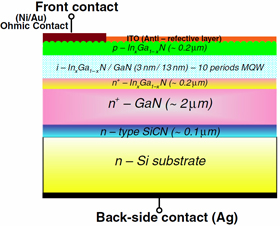 Figure: Schematic of InxGa1-xN/GaN-based solar cells with an MQW structure using SiCN/Si(111) substrate. The conducting indium tin oxide (ITO) has an anti-reflective coat to improve entry of light into the device.
For Liou’s devices, lower indium contents were found to give higher performance (Table) in terms of conversion efficiency (η), open-circuit voltage (Voc), short-circuit current (Jsc), and fill factor (FF = (maximum power)/(JscVoc)). This is attributed to the wider energy band gap of InGaN with lower indium content.
Type |
x |
Voc (V) |
Jsc(mA/cm2) |
FF (%) |
η, efficiency (%) at 28C |
0.94 |
2.83 |
38.1 |
88.7 |
30.1 |
|
p–n |
0.83 |
2.88 |
38.5 |
85.2 |
32.4 |
0.68 |
3.09 |
40.1 |
86.3 |
33.5 |
|
0.94 |
2.92 |
55.1 |
89.5 |
35.1 |
|
p–MQW–n |
0.83 |
2.96 |
55.8 |
90.4 |
36.4 |
0.68 |
3.16 |
56.5 |
91.8 |
38.5 |
Table: Parameters for InxGa1-xN devices with and without multi-quantum well region and various indium contents (x).
Liou believes that significant progress has been made towards application of the technology in a concentrator-solar cell module set-up.
![]() Search: InGaN MQW Solar cells
Search: InGaN MQW Solar cells
Visit: http://jjap.ipap.jp/link?JJAP/48/072201
The author Mike Cooke is a freelance technology journalist who has worked in the semiconductor and advanced technology sectors since 1997.
Comment
Since posting this news item, Bob Forcier (CEO of RoseStreet Labs, www.rosestreetlabs.com) has noted the following concerning the original article ‘High Photovoltaic Efficiency of InxGa1-xN/GaN-Based Solar Cells with a Multiple-Quantum-Well Structure on SiCN/Si(111) Substrates’ (Bor Wen Liou, Japanese Journal of Applied Physics, vol.48 p. 072201, 2009):
“The highest-efficiency cell with the open-circuit voltage of 3.16V, short-circuit current of 56.5mA/cm2 and fill factor 0.918 would produce a power of 0.164W from 1cm2 when illuminated with AM 1.5G solar spectrum. Since the incident power of the solar spectrum is only 0.1W/cm2, that would suggest a completely unrealistic power conversion efficiency of 164% rather than 38.5% listed in the paper.”
Semiconductor Today has contacted the author Bor Wen Liou for clarification, and will report any feedback when received.
![]() ©2009 Juno Publishing and Media Solutions Ltd. All rights reserved. Semiconductor Today and the editorial material contained within it and related media is the copyright of Juno Publishing and Media Solutions Ltd. Reproduction in whole or part without permission from Juno Publishing and Media Solutions Ltd is forbidden. In most cases, permission will be granted, if the author, magazine and publisher are acknowledged.
©2009 Juno Publishing and Media Solutions Ltd. All rights reserved. Semiconductor Today and the editorial material contained within it and related media is the copyright of Juno Publishing and Media Solutions Ltd. Reproduction in whole or part without permission from Juno Publishing and Media Solutions Ltd is forbidden. In most cases, permission will be granted, if the author, magazine and publisher are acknowledged.
Disclaimer: Material published within Semiconductor Today and related media does not necessarily reflect the views of the publisher or staff. Juno Publishing and Media Solutions Ltd and its staff accept no responsibility for opinions expressed, editorial errors and damage/injury to property or persons as a result of material published.
Semiconductor Today, Juno Publishing and Media Solutions Ltd, Suite no. 133, 20 Winchcombe Street, Cheltenham, GL52 2LY, UK
Web site by No Name No Slogan ![]()