| Home | About Us | Contribute | Bookstore | Advertising | Subscribe for Free NOW! |
| News Archive | Features | Events | Recruitment | Directory |
| FREE subscription |
| Subscribe for free to receive each issue of Semiconductor Today magazine and weekly news brief. |
News
2 February 2009
Following the thread of LED efficiency droop
The effect of threading dislocations on InGaN LED performance has been the subject of detailed investigations at the Fraunhofer-Institut für Angewandte Festkörperphysik (Fraunhofer-IAF, or Fraunhofer Institute for Applied Solid State Physics) [Maier et al, App. Phys. Lett., vol.94 (issue 4), p041103, 2009]. Of particular importance is finding the optimal conditions to reduce or eliminate the efficiency droop that occurs at high current density in such devices, limiting their effectiveness as high brightness light emitters.
The experimental work involved studying LEDs grown on sapphire and free-standing GaN substrates. GaN grown on sapphire with a low-temperature nucleation layer had a high dislocation density (high DD) of 109/cm2, as determined by etch-pit densities. An ultra-low dislocation (ULD) GaN on sapphire from France-based Lumilog showed a much reduced dislocation density of 8x10⁷/cm2, while a free-standing (FS) GaN substrate where the GaN material is separated from the sapphire to achieve even lower dislocation levels (also from Lumilog) had a density of 4x10⁷/cm2.
The LED devices were grown using metal-organic chemical vapor deposition (MOCVD) equipment from Aixtron. The precursors for the buffer and contact layers were trimethyl-gallium (TMGa), trimethyl-aluminum (TMAl), silane (SiH4), bis-cyclopentadienyl-magnesium (Cp2Mg) and ammonia (NH3) in a hydrogen (H2) gas carrier. The active layers were grown using triethyl- gallium (TEGa), trimethyl-indium (TMIn) and NH3 in 90:10 nitrogen:hydrogen gas.
The LED structures consisted of an Si-doped (1019/cm3) n-type contact layer followed by a single active well of InGaN of varying width (nominally 1.5nm, 3nm, 6nm, 11nm, 18nm), a non-doped 2nm GaN spacer layer, a 10nm Al0.1Ga0.9N electron blocker, and 100nm Mg-doped (6x10¹⁹/cm2) p-type GaN contact. High-resolution x-ray diffraction (HRXRD) was used to examine the quality of the devices, while photo- (PL) and electro-luminescence (EL) measurements were made to determine their optoelectronic performance. The EL current consisted of 1 microsecond pulse at a 0.1% duty cycle to avoid self-heating effects, focusing on the non-thermal roll-over/droop phenomenon. The HRXRD confirmed an In content of 9% and that even for the widest active layers of 18nm there was no relaxation. The PL emission was around 3.1eV (near-ultraviolet wavelength of 399nm).
The high-DD structure showed optimum performance for a 3nm well, while the ULD device operated best at 11nm. Free-standing GaN LEDs were continuing to improve at well widths of 18nm. At very narrow widths (e.g. at 1.5nm for the ULD LED) the devices are limited in output by the lack of confinement of carriers in the well due to the high quantization energies. At moderate widths, the emission efficiency increases rapidly with the current but then droops. Beyond the optimum width the droop is overcome but the maximum efficiency of the device is lower, particular for the high-DD LEDs. This is interpreted as being due to the increased recombination time due to lower carrier densities reducing its effectiveness over other non-radiative recombination processes.
 The authors point out that the external quantum efficiencies are not exactly comparable between the sapphire and free-standing devices. This is because the back surfaces of the of the sapphire devices have been roughened to improve light output, while the free-standing GaN LEDs have polished back surfaces.
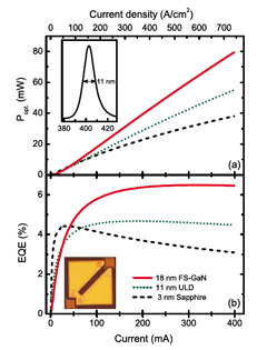
Figure: Output power (a) and external quantum efficiency (b) for mesa-structure LEDs. Inset top is the EL spectrum for 18nm free-standing GaN LED. Inset bottom is micrograph of mesa-structure.
To improve the characterization of current density performance, mesa-structure LEDs were also built using lithography and etch methods. The well widths were optimized for each base: 3nm for high-DD GaN/sapphire, 11nm for ULD GaN/sapphire, and 18nm for FS GaN. Also each device has a roughened back surface to improve comparability of output. However, differences in the refractive indices of sapphire and GaN were not taken into account. The EL spectrum for the 18nm free-standing device was centered on 402nm with a full-width at half-maximum of 11nm. The free-standing LEDs show no non-thermal roll-over/droop up to 750A/cm².
The researchers believe that the results point to an Auger-like mechanism for the roll-over/droop. This kicks in at high carrier densities and diverts recombination from light emission. The wider wells reduce the carrier densities. However, they also note that heterostructure simulations hint at a reduced carrier leakage linked to piezoelectric fields in wider-well LEDs.
The research was supported by Germany's Federal Ministry for Education and Research (BMBF) and by Osram Opto Semiconductors GmbH.
See related items:
RPI cuts LED efficiency droop via polarization-matched GaInN/GaInN MQWs
Fathoming efficiency droop in InGaN MQW-LEDs
See article: Solutions don’t solve droop controversy
![]() Search: LEDs Droop InGaN GaN substrates Sapphire substrates Aixtron MOCVD
Search: LEDs Droop InGaN GaN substrates Sapphire substrates Aixtron MOCVD
Visit: www.iaf.fraunhofer.de
Visit: http://apl.aip.org/apl
The author Mike Cooke is a freelance technology journalist who has worked in the semiconductor and advanced technology sectors since 1997.

![]() ©2009 Juno Publishing and Media Solutions Ltd. All rights reserved. Semiconductor Today and the editorial material contained within it and related media is the copyright of Juno Publishing and Media Solutions Ltd. Reproduction in whole or part without permission from Juno Publishing and Media Solutions Ltd is forbidden. In most cases, permission will be granted, if the author, magazine and publisher are acknowledged.
©2009 Juno Publishing and Media Solutions Ltd. All rights reserved. Semiconductor Today and the editorial material contained within it and related media is the copyright of Juno Publishing and Media Solutions Ltd. Reproduction in whole or part without permission from Juno Publishing and Media Solutions Ltd is forbidden. In most cases, permission will be granted, if the author, magazine and publisher are acknowledged.
Disclaimer: Material published within Semiconductor Today and related media does not necessarily reflect the views of the publisher or staff. Juno Publishing and Media Solutions Ltd and its staff accept no responsibility for opinions expressed, editorial errors and damage/injury to property or persons as a result of material published.
Semiconductor Today, Juno Publishing and Media Solutions Ltd, Suite no. 133, 20 Winchcombe Street, Cheltenham, GL52 2LY, UK
Web site by No Name No Slogan ![]()