| Home | About Us | Contribute | Bookstore | Advertising | Subscribe for Free NOW! |
| News Archive | Features | Events | Recruitment | Directory |
| FREE subscription |
| Subscribe for free to receive each issue of Semiconductor Today magazine and weekly news brief. |
News
1 December 2009
InGaN LED spillover and efficiency droop
Virginia Commonwealth University (VCU) has been studying the effects of polarization-induced fields and spillover effects in indium gallium nitride (InGaN) LEDs using m-plane gallium nitride substrates supplied by Kyma Technologies Inc of Raleigh, NC, USA. The aim of the research [Lee et al, Appl. Phys. Lett. vol95, p201113, 2009] is a better understanding of the cause of the severe efficiency droop in such devices that is often seen at operating current densities of more than 50A/cm2.
A number of explanations have been put forward for why the droop occurs. One of the most popular is that a non-radiative ‘Auger’ or Auger-like process is competing with the electron–hole recombination event that produces photons. An Auger process transfers the energy from the electron–hole recombination to another electron or hole (i.e. either eeh or ehh). Since three particles are involved, this process has roughly a cubic dependence on carrier densities, while the photon-producing electron–hole process has a two-particle square dependence. Hence, it is argued, as the current (and hence carrier density) increases, the Auger process will increasingly sap the ability of the LED to produce more light.
VCU takes a different position, based in part on theoretical work last year [Hader et al, Appl. Phys. Lett., vol92, p261103, 2008] that suggested that the Auger coefficient in wide-bandgap materials is too low to explain the efficiency droop in InGaN LEDs. One of the leaders of the VCU group, Hadis Morkoç, does not believe that this position is changed by more recent theoretical work showing an enhanced Auger coefficient when the InGaN semiconductor is such that its band gap is about 2.5eV due to resonant coupling with excited bands above the conduction band [Delaney et al, Appl. Phys. Lett., vol94, p191109, 2009]. Morkoç points out that this effect should mainly affect blue–green LEDs with wavelengths around 500nm, corresponding to photon energies of about 2.5eV. The emission wavelengths from the VCU devices were around 400nm (~3eV), which is well above the theoretical peak in Auger enhancement.
Instead of Auger effects, VCU has researched polarization and spillover. Polarization fields arise from the partly ionic nature of the bond between the components of nitride semiconductors with group III (Ga, In) and group V (N) elements. Both spontaneous and piezoelectric (strain-dependent) electric fields arise from such polarization. These fields can adversely affect the performance of both LEDs and laser diodes. Polarization fields are the favored explanation for efficiency droop advocated by the group at Rensselaer Polytechnic Institute (RPI) led by Fred Schubert.
Electron spillover is where electrons pass through the region where light emission is supposed to occur and reach the p-type upper layers of the device. The presence of magnesium doping to create high hole carrier densities tends also to increase non-radiative Shockley–Read–Hall recombination through intermediate levels in the band gap. One of the possible effects of polarization may be to increase the level of this spillover. Hole spillover in the opposite direction is much less likely, due to lower mobility and difficulties in producing high p-type carrier levels in nitride semiconductors.
To investigate these effects, the researchers used m-plane GaN substrates supplied by Kyma to remove the polarization fields that are seen in devices grown in the c-plane direction. Similar m-plane substrates have also recently achieved prominence in research attempting to fill the green gap for laser diodes based on InGaN structures.
The m-plane substrates were obtained by cutting c-plane GaN crystals in a direction perpendicular to the surface (slightly offcut by 0.2° towards the a-axis and 0.3° to the c-axis). The c-plane crystals were grown using hydride vapor phase epitaxy (HVPE). For comparison, devices were also produced on c-plane GaN on sapphire substrates using traditional metal-organic chemical vapor deposition (MOCVD).
The light-emitting layers consisted of six periods of 2nm thick In0.14Ga0.86N wells with 12nm thick In0.01Ga0.99N. Some of the devices included electron-blocking layers (EBLs) designed to reduce the number of electrons reaching the p-type GaN layers. The EBL consisted of ~10nm-thick Mg-doped
p-Al0.15Ga0.85N.
Photoluminescence (PL) studies with 370nm radiation from a frequency-doubled Ti:sapphire laser show increasing internal quantum efficiency (i.e. more radiative recombination relative to non-radiative) with excited carrier density. The m-plane structures had up to 80–85% more emissions compared with the c-plane structures.
The m-plane structure with EBL was slightly less luminescent than the one without EBL. VCU attributes this to variations in quality of the m-plane GaN substrates. However, compared with material grown on sapphire, the m-plane material would be expected to have better quality and hence better PL behavior. In addition, light couples better in the m-plane direction. The lack of effect of the EBL on optical measurements suggests to the VCU researchers that the polarization fields in the c-plane substrate do not have a significant impact on spillover.
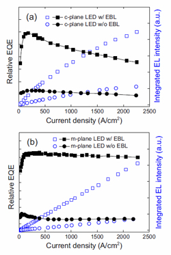 VCU then subjected the LEDs to various currents to obtain electroluminescence information (Figure 1). A pulsed current source with a 0.1% duty cycle and 1kHz frequency was used to avoid heating effects. The EBL is seen to give much better external quantum efficiency (EQE) in both c-plane and m-plane devices for low currents. The c-plane LEDs with EBL have a severe fall-off for large current densities (~40% for 2250 A/cm2 with EBL). The m-plane EBL sample has negligible droop.
Figure 1: Values for relative EQE (solid symbols) and light intensity (open symbols) of c-LEDs (a) and m-LEDs (b) with and without EBL as a function of current density applied by a 0.1% duty cycle pulsed current source. Measurements were made without any dicing or packaging.
Without EBL, both samples have peak efficiencies of about 20% of the comparable sample with EBL. Degradation of efficiency at higher currents is ‘strikingly absent’ in the c-plane sample without EBL, while the m-plane sample settles at a constant lower value. The cause of the peak in the m-plane LED is under investigation.
“Because the relative EQE remains nearly constant for most of the current range investigated in the m-plane variety, we can also argue that the spillover is linearly proportional to the drive current,” the authors conclude.
VCU suggests that increasing the p-doping in the upper layers and/or reducing the n-doping in the layers below the MQW could reduce the electron spillover effects by ensuring radiative recombination of the electrons and holes in the undoped MQW before they enter the p-type or n-type regions.
See related items:
New angle on approach to green lasers
Non-polar InGaN lasers near green light
See article: Getting a green light from lasers
![]() Search: InGaN LEDs GaN substrates Kyma
Search: InGaN LEDs GaN substrates Kyma
Visit: http://link.aip.org/link/?APPLAB/95/201113/1
Visit: http://link.aip.org/link/?APPLAB/92/261103/1
Visit: http://link.aip.org/link/?APPLAB/94/191109/1The author Mike Cooke is a freelance technology journalist who has worked in the semiconductor and advanced technology sectors since 1997.
![]() ©2009 Juno Publishing and Media Solutions Ltd. All rights reserved. Semiconductor Today and the editorial material contained within it and related media is the copyright of Juno Publishing and Media Solutions Ltd. Reproduction in whole or part without permission from Juno Publishing and Media Solutions Ltd is forbidden. In most cases, permission will be granted, if the author, magazine and publisher are acknowledged.
©2009 Juno Publishing and Media Solutions Ltd. All rights reserved. Semiconductor Today and the editorial material contained within it and related media is the copyright of Juno Publishing and Media Solutions Ltd. Reproduction in whole or part without permission from Juno Publishing and Media Solutions Ltd is forbidden. In most cases, permission will be granted, if the author, magazine and publisher are acknowledged.
Disclaimer: Material published within Semiconductor Today and related media does not necessarily reflect the views of the publisher or staff. Juno Publishing and Media Solutions Ltd and its staff accept no responsibility for opinions expressed, editorial errors and damage/injury to property or persons as a result of material published.
Semiconductor Today, Juno Publishing and Media Solutions Ltd, Suite no. 133, 20 Winchcombe Street, Cheltenham, GL52 2LY, UK
Web site by No Name No Slogan ![]()