| Home | About Us | Contribute | Bookstore | Advertising | Subscribe for Free NOW! |
| News Archive | Features | Events | Recruitment | Directory |
| FREE subscription |
| Subscribe for free to receive each issue of Semiconductor Today magazine and weekly news brief. |
News
17 December 2009
Progress towards high-efficiency InGaN/Si tandem solar cell
The US Lawrence Berkeley National Laboratory (LBNL) and RoseStreet Labs Energy (RSLE) have jointly reported the development of a gallium nitride/silicon (GaN/Si) tandem solar cell [Reichertz et al, Appl. Phys. Express, vol2, p122202, 2009]. The aim of the ‘proof-of-principle’ device (Figure 1) is to enable use of the bandgap characteristics of two materials to pick up energy from different energy photons in solar radiation, boosting efficiency.
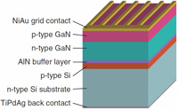 Figure 1: GaN/Si tandem solar cell prototype.
Pure GaN is not ideal for this purpose since very little solar radiation falls in the energy range of its bandgap, meaning that the efficiency of a GaN/Si tandem device is limited to around 1.5% under the standard 1x AM1.5G solar radiation testing conditions. This is worse than if one made a single-junction Si solar cell (for which more than 20% is possible).
The problem with the pure-GaN structure is that carrier generation is low, given the low level of (ultraviolet) radiation in the solar spectrum with photon energies above the bandgap. The result is low generated current density. Since the GaN part of the device is connected in series with the Si part, the current performance of the device as a whole is limited to that of the GaN portion.
The hope is to narrow the gap of the top semiconductor by adding indium to create InGaN with a suitable bandgap that matches the requirements of solar radiation, giving efficiencies nearing 30%. Such work by the researchers at RSLE and LBNL on incorporating In is described as ‘ongoing’.
The pure-GaN device structure was produced on n-type silicon (111) substrates using plasma-assisted molecular beam epitaxy (PA-MBE). A buffer layer of aluminum nitride was used to bridge the large lattice mismatch of about 17% between GaN and Si. An interesting by-product of the AlN layer is that some Al diffuses into the Si, producing a p-type Al-doped region in the silicon, forming the Si part of the solar cell. The grown GaN layer is n-type until a magnesium source is turned on to produce p-type GaN material.
A low-resistance tunnel junction between the two cells is needed if such a structure is to be effective. The researchers confirmed a total series resistance of 0.5Ω-cm2 by characterizing a device with no p-type GaN layer. The efficiency of this truncated device was ~9%.
The full device had a measured efficiency below 1% at 1x AM1.5G. The open-circuit voltage (Voc) was 1.44V (2.5x that of the Si bottom cell), but the short-circuit current density (Jsc)was only 0.16mA/cm2. The fill factor (maximum power/VocxIsc) was 40%.
Increased Voc (2.4V) is possible by adding a monochromatic light bias source above the bandgap of GaN to increase carrier generation in the top cell (Figure 2).
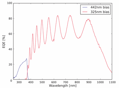
Figure 2: External quantum efficiency (EQE) spectra of pn-GaN/pn-Si tandem solar cell under different bias light conditions. Monochromatic bias light is used to separately measure each sub cell. Biasing the Si sub cell with 442nm wavelength allows scanning of the EQE spectrum of the GaN cell, while the shorter wavelength 325nm falls above the GaN band gap, biasing the top cell only, enabling measurement of the EQE of the silicon cell. Note the Fabry-Perot oscillations in the sub-cell spectrum from interference between various reflections from the interfaces by the light in the GaN layer, indicating the high optical quality of the GaN surface.
RSLE claims intellectual property rights over the technology.
See related item:
![]() Search: Lawrence Berkeley RoseStreet GaN/Si tandem solar cell InGaN
Search: Lawrence Berkeley RoseStreet GaN/Si tandem solar cell InGaN
Visit: http://apex.ipap.jp/link?APEX/2/122202
Visit: www.rosestreetlabs.com
The author Mike Cooke is a freelance technology journalist who has worked in the semiconductor and advanced technology sectors since 1997.
![]() ©2009 Juno Publishing and Media Solutions Ltd. All rights reserved. Semiconductor Today and the editorial material contained within it and related media is the copyright of Juno Publishing and Media Solutions Ltd. Reproduction in whole or part without permission from Juno Publishing and Media Solutions Ltd is forbidden. In most cases, permission will be granted, if the author, magazine and publisher are acknowledged.
©2009 Juno Publishing and Media Solutions Ltd. All rights reserved. Semiconductor Today and the editorial material contained within it and related media is the copyright of Juno Publishing and Media Solutions Ltd. Reproduction in whole or part without permission from Juno Publishing and Media Solutions Ltd is forbidden. In most cases, permission will be granted, if the author, magazine and publisher are acknowledged.
Disclaimer: Material published within Semiconductor Today and related media does not necessarily reflect the views of the publisher or staff. Juno Publishing and Media Solutions Ltd and its staff accept no responsibility for opinions expressed, editorial errors and damage/injury to property or persons as a result of material published.
Semiconductor Today, Juno Publishing and Media Solutions Ltd, Suite no. 133, 20 Winchcombe Street, Cheltenham, GL52 2LY, UK
Web site by No Name No Slogan ![]()