| Home | About Us | Contribute | Bookstore | Advertising | Subscribe for Free NOW! |
| News Archive | Features | Events | Recruitment | Directory |
| FREE subscription |
| Subscribe for free to receive each issue of Semiconductor Today magazine and weekly news brief. |
News
4 August 2009
New angle on approach to green lasers
Shuji Nakamura’s group at University of California Santa Barbara (UCSB) has reported on a blue-green laser diode (LD) based on a miscut m-plane gallium nitride (GaN) substrate [You-Da Lin et al, Applied Physics Express, vol.2, p.082102, 2009]. Nakamura is responsible for much of the development and commercialization of GaN as a light emitting material for electronics as part of Nichia Corporation in Japan in the late 1980s and all through the 1990s until he became a UCSB professor in 1999. Also involved in the research is a researcher from Mitsubishi Chemical’s Optoelectronics Laboratory, Kenji Fujito, who has worked on hydride vapor phase epitaxy (HVPE) of high quality non-polar m-plane GaN substrates [Kenji Fujito et al, physica status solidi (a), vol.205, p.1056, 2007].
While producing red and blue laser light from semiconductors is relatively simple, producing green lasers has been much harder. At present, green laser light (520-570nm) in commercial LD-based systems, such as overhead projectors, is most often produced using conversion from sources emitting another frequency via second harmonic generation (SHG).
This year has seen a number of groups publish paper describing various approaches to producing green lasers in the III-nitride material system with indium gallium nitride (InGaN) active layers. In February, Rohm pushed InGaN laser wavelengths out to 499.8nm; in March, Osram Opto Semiconductors crossed the 500nm boundary; and then, in May, Nichia Corp. announced a 515nm device.
These developments use various techniques to improve material quality, which is particularly key for the active layer where indium concentrations have to exceed 20% to achieve suitable energy band gaps to produce green light. High indium content InGaN is notoriously difficult to grow with the high quality demanded from laser applications.
Although the UCSB work has only reached 481nm so far, the researchers point to improved performance by using miscut non-polar substrates in terms of lasing threshold currents and slope efficiency that suggest moving to longer wavelengths should be “easy” and a possible route to realizing high power green LDs.
Normally LDs are grown on c-plane GaN, but large polarization fields arise. Such fields separate the electron and hole wave-functions, reducing their ability to radiate light by recombination. An advantage of m-plane GaN is that it is non-polar. Violet m-plane GaN LDs were reported in 2007 and also were the basis of Rohm’s work. One problem for c-plane LDs in the blue-green region has been low slope efficiency. Devices using m-plane substrates demonstrate better slope efficiency than those grown on c-plane GaN, meaning that more of the extra power delivered beyond the threshold becomes laser light.
For the UCSB LDs, the m-plane GaN substrate was miscut about 1° in the [000-1] (-c) direction. Miscutting of substrates is commonly used to improve or manipulate material quality on a wide range of substrates. [For a recent example involving improving quantum dot shapes and sizes on an indium phosphide (InP) substrate, see Optimizing InP substrate orientation for 1.55µm InAs QD telecom lasers].
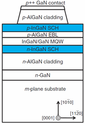 UCSB used metal organic chemical vapor deposition (MOCVD) to grow the LD. The active layer was a three-period multi-quantum well (10 nm undoped In0:03Ga0:97N barriers, 3nm InGaN wells with ~26% In estimated through high resolution x-ray diffraction). Electron blocking layers (EBLs) and separate confinement heterostructures (SCHs) were also used (Figure 1).
Figure 1. Schematic of laser diode structure used by UCSB. SCH = separate confinement heterostructure. EBL = electron blocking layer.
Ridge lasers pointing in the c-direction were formed using normal photolithography and etch processes. Nomarski and fluorescence optical microscopy of LD surfaces grown on nominal on-axis and miscut substrates showed significantly smoother surface without “hillocks” for the LD on miscut substrate. Also photoluminescence was much more homogeneous for the miscut substrate device.
A comparison of 2x500μm LDs with uncoated facets in pulsed operation (1% duty cycle) show a lower threshold current (153mA, compared with 413mA for nominal on-axis device), for the miscut substrate. Further, less blue shift was seen in moving from spontaneous to laser emission (~483nm spontaneous wavelength for both miscut and nominal, 471nm miscut lasing, 461nm on-axis lasing). These properties are attributed to larger indium fluctuations in the on-axis samples. A clarification of the mechanisms is promised in a future publication from the group.
The threshold current density tends to increase with wavelength (Figure), but with the miscut devices generally reporting a lower value. The longest lasing wavelength found was 481nm (10nm from spontaneous photoluminescence at 491nm) from a coated facet device in 1% duty pulsed operation.
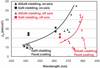
Figure 2. Dependence of threshold current density on lasing wavelength for various laser diodes produced by UCSB using on-axis and 1° towards [000-1] direction misoreinted substrates.
See related items:
Sumitomo Electric claims first pure-green semiconductor laser
Nichia pushes InGaN lasers nearer to green via 515nm emission
Osram Opto claims first 500nm InGaN laser
Non-polar InGaN lasers near green light
![]() Search: Green laser InGaN
Search: Green laser InGaN
Visit: http://apex.ipap.jp/link?APEX/2/082102/
Visit: http://dx.doi.org/10.1002/pssa.200778709
The author Mike Cooke is a freelance technology journalist who has worked in the semiconductor and advanced technology sectors since 1997.
![]() ©2009 Juno Publishing and Media Solutions Ltd. All rights reserved. Semiconductor Today and the editorial material contained within it and related media is the copyright of Juno Publishing and Media Solutions Ltd. Reproduction in whole or part without permission from Juno Publishing and Media Solutions Ltd is forbidden. In most cases, permission will be granted, if the author, magazine and publisher are acknowledged.
©2009 Juno Publishing and Media Solutions Ltd. All rights reserved. Semiconductor Today and the editorial material contained within it and related media is the copyright of Juno Publishing and Media Solutions Ltd. Reproduction in whole or part without permission from Juno Publishing and Media Solutions Ltd is forbidden. In most cases, permission will be granted, if the author, magazine and publisher are acknowledged.
Disclaimer: Material published within Semiconductor Today and related media does not necessarily reflect the views of the publisher or staff. Juno Publishing and Media Solutions Ltd and its staff accept no responsibility for opinions expressed, editorial errors and damage/injury to property or persons as a result of material published.
Semiconductor Today, Juno Publishing and Media Solutions Ltd, Suite no. 133, 20 Winchcombe Street, Cheltenham, GL52 2LY, UK
Web site by No Name No Slogan ![]()