| Home | About Us | Contribute | Bookstore | Advertising | Subscribe for Free NOW! |
| News Archive | Features | Events | Recruitment | Directory |
| FREE subscription |
| Subscribe for free to receive each issue of Semiconductor Today magazine and weekly news brief. |
News
17 April 2009
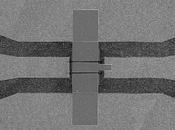
Glasgow shrinks diamond transistor to 50nm
Researchers at the University of Glasgow have developed what is claimed to be the world’s smallest diamond transistor. Developed by Dr David Moran of the Department of Electronics & Electrical Engineering, the transistor's gate is just 50nm long. This is half the size of the previous smallest diamond transistor, which was developed by Japanese firm NTT.
Due to its unique and highly desirable material properties (such as large bandgap, high intrinsic mobility, and very high thermal conductivity), diamond is regarded as an ideal material for next-generation nanoscale electronic devices and could help the development of nascent technologies such as terahertz imaging and automotive collision detection.
Terahertz imaging uses terahertz radiation (T-rays, with a frequency between that of microwaves and infrared), which can penetrate a range of materials (including clothes and flesh) to create an image. Because it is non-ionizing, it does not damage cells and has potential applications to security scanners (e.g. for detecting concealed weapons) as well as to safer medical imaging.
 The car industry is developing automotive collision detection (or automotive radar) as a safety feature in which a vehicle has an effective radar zone around it that allows it to detect potential collisions (from any side) well in advance and then take avoiding action.
Picture: Glasgow's 50nm-gate diamond transistor.
“These applications require a very fast and ideally high-power transistor technology that needs to be able to operate in adverse weather/temperature conditions,” says Moran. “This is where a diamond transistor technology would excel”.
The diamond material that was used in the device is made synthetically, using chemical vapor deposition, by Element Six Ltd of Ascot, UK (via its subsidiary Diamond Microwave Devices). Fabrication of the device is part of a five-year project ‘Ultra short gate length diamond FETs for high power/high frequency applications’ (lasting from October 2007 to September 2012) funded with £0.5m from the UK Engineering & Physical Sciences Research Council (EPSRC). It is also the result of collaborative work between Heriot Watt University and the University of Glasgow, using the extensive fabrication and characterization facilities within the latter’s James Watt Nanofabrication Centre (including an ultra-high-resolution Vistek VB6 electron-beam lithography tool).
![]() Search: Diamond transistor Terahertz imaging
Search: Diamond transistor Terahertz imaging
Visit: www.elec.gla.ac.uk

![]() ©2009 Juno Publishing and Media Solutions Ltd. All rights reserved. Semiconductor Today and the editorial material contained within it and related media is the copyright of Juno Publishing and Media Solutions Ltd. Reproduction in whole or part without permission from Juno Publishing and Media Solutions Ltd is forbidden. In most cases, permission will be granted, if the author, magazine and publisher are acknowledged.
©2009 Juno Publishing and Media Solutions Ltd. All rights reserved. Semiconductor Today and the editorial material contained within it and related media is the copyright of Juno Publishing and Media Solutions Ltd. Reproduction in whole or part without permission from Juno Publishing and Media Solutions Ltd is forbidden. In most cases, permission will be granted, if the author, magazine and publisher are acknowledged.
Disclaimer: Material published within Semiconductor Today and related media does not necessarily reflect the views of the publisher or staff. Juno Publishing and Media Solutions Ltd and its staff accept no responsibility for opinions expressed, editorial errors and damage/injury to property or persons as a result of material published.
Semiconductor Today, Juno Publishing and Media Solutions Ltd, Suite no. 133, 20 Winchcombe Street, Cheltenham, GL52 2LY, UK
Web site by No Name No Slogan ![]()