| Home | About Us | Contribute | Bookstore | Advertising | Subscribe for Free NOW! |
| News Archive | Features | Events | Recruitment | Directory |
| FREE subscription |
| Subscribe for free to receive each issue of Semiconductor Today magazine and weekly news brief. |
News
15 September 2008
New wafer slicing method cuts waste in making Ge-based solar cells
Following work funded by the US National Science Foundation, the University of Utah Research Foundation and germanium wafer maker Sylarus Technologies of St George, UT, USA, researchers at the University of Utah have reported a new method for slicing thin germanium wafers that could lower the cost of solar cells by reducing the waste and breakage of the brittle substrate (to be published next year in Journal of Materials Processing Technology).
Germanium is used as both the substrate and the bottom of a multi-junction solar cells, upon which layers of gallium indium arsenide (GaInAs) and gallium indium phosphide (GaInP) are grown to produce the other junctions. Such solar cells are currently used mainly on spacecraft, but the idea is to make germanium-based, high-efficiency solar cells for uses where cost now is a factor, particularly for terrestrial (e.g. roof-based) solar power, says assistant professor of mechanical engineering Eberhard ‘Ebbe’ Bamberg.
Bamberg says that germanium-based solar cells are used on most spacecraft because they are more efficient and lighter than silicon-based solar cells. Silicon-based terrestrial solar cells have maximum efficiency of 20%. In space, germanium-based solar cells typically convert 28% of sunlight into electricity, but on Earth (e.g. in solar concentrators) they can have an efficiency of more than 40%, and theoretically exceed 50%. But despite the greater efficiency, a 2005 survey found that 94% of solar cells made for non-space uses were silicon-based, because silicon is much cheaper and less fragile than germanium.
"We're coming up with a more efficient way of making germanium wafers for solar cells – to reduce the cost and weight of these solar cells and make them defect-free," says doctoral student Dinesh Rakwal. The new method may make germanium-based solar cells competitive with less efficient but less expensive silicon-based solar cells for terrestrial applications, believes Bamberg. By making it more attractive economically to use efficient germanium solar cells on rooftops, the weight and size of solar panels can be reduced "so it doesn't bother you aesthetically," he adds.
Traditionally, brass-coated, steel-wire saws are used to slice germanium wafers from cylindrical single-crystal ingots. However, since germanium is brittle, it cracks easily, requiring broken pieces to be recycled. Also, the width of the saw means that a significant amount of germanium is lost during slicing. The sawing method was developed for silicon wafers, which are about 100 times stronger.
The new slicing method – wire electrical discharge machining (WEDM) – wastes less germanium and produces more wafers by cutting even thinner wafers with less waste and cracking, say the researchers. The method - which has previously been used for machining metals during tool-making - uses an extremely thin molybdenum wire with an electrical current running through it, essentially forming an electrode.
 This is connected to a pulsed power supply that charges the wire during the cutting process. Thin, synthetic oil is injected along the wire, both to increase the electrical charge on the wire and to flush away material that melts during the cutting process.
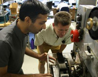
Picture: Dinesh Rakwal and Eberhard Bamberg watch as an electrified molybdenum wire cuts a thin germanium wafer. Credit: Sumet Heamawatanachai, University of Utah.
Wire electrical discharge machining takes 14 hours to cut a single wafer. The electrified wire method has to be conducted gently to avoid cracking the germanium, but Bamberg hopes to increase the speed to the six hours it now takes to cut a wafer using a wire saw.
Compared to wire saws made of brass-coated steel with a thickness of about 170 or 180 microns, the molybdenum wire is just 75-100 microns thick, so less germanium is wasted during the slicing process. The study found that a 100 micron-thick electrified wire significantly reduced the waste and increased the number of wafers that could be made from a germanium ingot. A thinner 75 micron-wide wire did even better. "At the current standard wafer thickness of 300 microns, you can produce up to 30% more wafers using our method with a 75 micron-wide wire", says Bamberg. "Since we produce them crack free, we can also make them thinner than standard techniques. So if you go down to a 100 micron-thick wafer, you can make up to 57% more wafers [from the same germanium ingot]." Making the wafers thinner will reduce their cost because more can be made from the same ingot, he adds.
The new study found that the kerf (the amount of germanium wasted during the slicing process) was 22% less when a 75 micron-wide electrified wire was used, compared with the conventional wire saw method. The researchers cut 2.6 inch-diameter wafers with a thickness of 350 microns.
The study also showed that less germanium was wasted not only using the smaller wire size, but also if the charge on the electrified wire was lower.
Germanium-based solar cell are used primarily on NASA, military and commercial satellites because of the high expense – raw germanium costs about $680 per pound. The 4-inch diameter wafers that are used cost $80-100 each. The new cutting method may reduce the cost by more than 10%, says Sylarus' chief technology officer Grant Fines. Anything that can be done to lower this cost ultimately will lower the cost of solar power per kilowatt-hour and encourage wider use of solar power, he adds.
Sylarus is considering using the new method, but must determine if it can be scaled up so that wafers can be mass-produced in a commercially viable manner, Fines says. Bamberg's method would "reduce the amount we have to recycle and increase the yield," he adds.
 A patent is pending on a way of using the new method so that multiple, parallel electrically charged wires can be used to cut germanium wafers in mass-production.
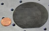
Picture: Germanium wafer cut from an ingot. Credit: Eberhard Bamberg.
Search: Germanium Germanium substrates Multi-junction solar cells GaInP
Visit: www.unews.utah.edu
![]()
![]() ©2008 Juno Publishing and Media Solutions Ltd. All rights reserved. Semiconductor Today and the editorial material contained within it and related media is the copyright of Juno Publishing and Media Solutions Ltd. Reproduction in whole or part without permission from Juno Publishing and Media Solutions Ltd is forbidden. In most cases, permission will be granted, if the author, magazine and publisher are acknowledged.
©2008 Juno Publishing and Media Solutions Ltd. All rights reserved. Semiconductor Today and the editorial material contained within it and related media is the copyright of Juno Publishing and Media Solutions Ltd. Reproduction in whole or part without permission from Juno Publishing and Media Solutions Ltd is forbidden. In most cases, permission will be granted, if the author, magazine and publisher are acknowledged.
Disclaimer: Material published within Semiconductor Today and related media does not necessarily reflect the views of the publisher or staff. Juno Publishing and Media Solutions Ltd and its staff accept no responsibility for opinions expressed, editorial errors and damage/injury to property or persons as a result of material published.
Semiconductor Today, Juno Publishing and Media Solutions Ltd, Suite no. 133, 20 Winchcombe Street, Cheltenham, GL52 2LY, UK
Web site by No Name No Slogan ![]()