| Home | About Us | Contribute | Bookstore | Advertising | Subscribe for Free NOW! |
| News Archive | Features | Events | Recruitment | Directory |
| FREE subscription |
| Subscribe for free to receive each issue of Semiconductor Today magazine and weekly news brief. |
News
2 May 2008
Broad-spectrum QCLs and GaAs nanoneedles
Among the promised highlights at the upcoming Conference on Lasers and Electro-Optics (CLEO) in San Jose, California (4-9 May) are compact arrays of 32 quantum cascade lasers (QCLs) and pure wurtzite GaAs nanoneedles.
Compactified QCL chemical sensors
Applications for which quantum cascade lasers (QCLs) have been proposed include acting as a source for various spectral measurements with a view to chemical detection. This is because QCLs offer compact access to regions of the infrared electromagnetic spectrum that previously required relatively large light sources. Last year, Harvard University researchers presented at CLEO on an array of 16 broadly tunable single-mode QCLs. This year’s contribution (with Agilent Labs) is on an array of 32 QCLs [Lee et al, CLEO Talk CMH1; “Continuously Tunable Compact Single-Mode Quantum Cascade Laser Source for Chemical Sensing"]. The center wavelength of the new 32-QCL array is 9 microns and the tuning range is 8% of this. Last year’s 16-QCL array emitted in the range 6.7-7.2 microns (or 1400-1490cm -1 in wavenumbers, as given in the paper; the range represented about 7% of the center wavelength). The individual QCLs can be tuned using the wavelength-temperature dependence of the device to cover the full range of the array.
The new 32-QCL array is ‘smaller than a dime’ in size. Presumably, the conference paper will go into more detail on this. Last year’s paper shows the 16-QCL array being of the order of a dime’s “In God We Trust” text – i.e. a very small part of the coin! The research team reports that the new source has been integrated into a compact mid-infrared spectrometer that could fit into a  shoebox for absorption spectroscopy of liquids and gases. Infrared spectrometry has applications in detection of toxic waste; the possibility of sniffing out ‘chemical weapons’ is also mentioned.
Picture: Array of 16 QCLs presented at last year's CLEO compared with a dime
coin.
Defect-free GaAs nanoneedles on silicon
University of California at Berkeley (UCB)’s GaAs nanoneedles have produced “bright photoluminescence” on optical pumping, according to the researchers [Moewe et al, CLEO/QLS Talk CTuCC1; “Bright Photoluminescence from GaAs and InGaAs Nanoneedles Grown on Si Substrates”]. However, laser action has not yet been produced – that is the next step in the research. The needles are 3‑4 microns in length, tapering at angles of 6‑9 degrees down to tips 2‑5nm across.
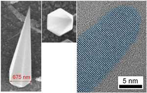
Picture: SEM (30° tilt and top-down, Si substrate) and TEM ([1-100] zone axis,
GaAs substrate) images of GaAs nanoneedles.
This is claimed as the first time a lab has been able to create defect-free GaAs wurtzite crystal needles like this on a silicon substrate and without the use of catalysts. UCB uses metal-organic chemical vapor deposition (MOCVD) process on both Si and GaAs substrates with a much lower growth temperature (~150Cº) than normal (>500ºC).
The usual GaAs crystal arrangement is the zincblende structure. Often in the growth of GaAs nanoneedles one finds a stacking switch occurs between wurtzite and zincblende. UCB says that it is the first to observe a pure wurtzite arrangement for GaAs nanowires.
The crystal lattice mismatch between gallium arsenide and silicon is around 4%. When GaAs nanowire diameters are limited to less than 100nm, defects arising from lattice mismatches can avoided by relaxing in two dimensions to relieve strain. UCB’s nanoneedles, however, can be grown up to a micron in diameter in a single-crystal phase, free of the twin defects that lead to wurtzite-zincblende switching.
The researchers hope that direct bandgap GaAs nanoneedles on silicon could be used to integrate traditional optoelectronic semiconductor devices directly with silicon circuits. The present goal is to demonstrate diode lasers on silicon. Reversing the direction to light-electron interactions, the structures could be used for efficient photo-detection on silicon, allowing for chip-scale optical communication systems, avoiding electrical signal limitations at high bandwidths.
In addition to optoelectronic devices, lead researcher Michael Moewe expects the needles to be valuable in such applications as atomic force microscopy (AFM), as the sharp tips can be grown in arrays without further etching or processing steps. AFM arrays can be used to speed up near-atomic level imaging. A further application could be to produce memory devices based on the ability of AFM tips to manipulate atoms on a surface.
Tip-enhanced Raman spectroscopy, measuring interactions between light and vibrational levels of materials, is another possible direction for development of the needles. Light from the sharp tips could give more targeted examination of samples, possibly to the single-molecule level. The optical signal is dependent on the square of the electric field generated at the probe tip – sharper tips greatly increase the intensity of the field.
Search: Quantum cascade lasers GaAs
Visit: www.cleoconference.org
Visit: www.seas.harvard.edu/capasso
Visit: http://light.eecs.berkeley.edu/cch/nanoneedles.html
The author Mike Cooke is a freelance technology journalist who has worked in the semiconductor and advanced technology sectors since 1997.
![]()
![]() ©2008 Juno Publishing and Media Solutions Ltd. All rights reserved. Semiconductor Today and the editorial material contained within it and related media is the copyright of Juno Publishing and Media Solutions Ltd. Reproduction in whole or part without permission from Juno Publishing and Media Solutions Ltd is forbidden. In most cases, permission will be granted, if the author, magazine and publisher are acknowledged.
©2008 Juno Publishing and Media Solutions Ltd. All rights reserved. Semiconductor Today and the editorial material contained within it and related media is the copyright of Juno Publishing and Media Solutions Ltd. Reproduction in whole or part without permission from Juno Publishing and Media Solutions Ltd is forbidden. In most cases, permission will be granted, if the author, magazine and publisher are acknowledged.
Disclaimer: Material published within Semiconductor Today and related media does not necessarily reflect the views of the publisher or staff. Juno Publishing and Media Solutions Ltd and its staff accept no responsibility for opinions expressed, editorial errors and damage/injury to property or persons as a result of material published.
Semiconductor Today, Juno Publishing and Media Solutions Ltd, Suite no. 133, 20 Winchcombe Street, Cheltenham, GL52 2LY, UK
Web site by No Name No Slogan ![]()