| Home | About Us | Contribute | Bookstore | Advertising | Subscribe for Free NOW! |
| News Archive | Features | Events | Recruitment | Directory |
| FREE subscription |
| Subscribe for free to receive each issue of Semiconductor Today magazine and weekly news brief. |
News
27 June 2008
JPSA enters thin-film PV scribing market
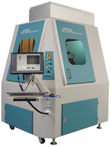
 J. P. Sercel Associates (JPSA) of Manchester, NH, USA has begun selling its new PV-5000 laser workstation, which is dedicated to scribing thin-film photovoltaic (PV) products. The first system deliveries to global PV product manufacturers are scheduled for fourth-quarter 2008.
The firm says that PV-5000 systems have the ability to laser machine high-efficiency thin-film PV panels, which cost significantly less to manufacture than existing silicon-based PV panels.
The increasing cost of silicon has spawned new ventures exploiting thin-film approaches for manufacturing photovoltaic panels. “New developments in PV film technology, coupled with the higher accuracy of laser scribing and edge deletion, have increased the electrical output of these new types of solar cells,” says CEO Jeffrey Sercel. “Their lower comparative cost to silicon-based solar cells, and the ability to manufacture them in larger panels, make them more accessible to an increasingly energy-hungry world.”
Thin-film scribing is an emerging PV manufacturing method that JPSA, with its well-developed wafer scribing business and technologies, is suited to entering, reckons Sercel. JPSA claims that its ChromaDice systems produce high-efficiency LEDs and provide higher yields per wafer than any other LED wafer scriber available.
The PV-5000 Thin Film PV Scribing System is based on the ChromaDice DPSS laser platform and is designed for isolation and series interconnection of thin-film solar cells. JPSA laser systems employ high-peak-power, short-pulsed diode-pumped solid-state (DPSS) laser sources to rapidly, selectively and accurately remove a wide range of thin films from large glass, metal or polymer substrates. A variety of wavelengths suitable for different layer materials are available, including 1064, 532, 355 and 266nm. The systems used laser technology scribing to rapidly and accurately produce fine scribed lines with virtually no heat affected zone (HAZ) and >30MOhm isolation.
See related items:
JPSA enhances laser-based automated wafer processing systems
JPSA awarded LED wafer scribing patent
Search: JPSA Thin-film photovoltaic LEDs
Visit: www.jpsalaser.com