


- News
5 December 2019
Self-aligned-gate gallium oxide metal-oxide-semiconductor transistors
Researchers based in the USA and Germany claim the first demonstration of self-aligned gate (SAG) β-polytype gallium oxide (β-Ga2O3) metal-oxide-semiconductor field-effect transistors (MOSFETs) [Kyle J. Liddy et al, Appl. Phys. Express, vol12, p126501, 2019].
The researchers at KBR Inc and the Air Force Research Laboratory in the USA and Leibniz-Institut für Kristallzüchtung (IKZ) in Germany used a refractory metal gate-first design with silicon (Si) ion-implantation to eliminate source access resistance, giving some of the highest transconductance values reported so far for β-Ga2O3 MOSFETs. The US part of the team was sited at the Wright-Patterson Air-Force Base, Ohio.
The researchers see such a SAG process as being “essential for future β-Ga2O3 device engineering to achieve high-performance, ultra-low-power-loss devices”.
It is only recently that β-Ga2O3 has been seriously considered as a semiconductor material for use in high-efficiency power applications, based on its ultra-wide bandgap (~4.8eV). The related high estimated critical field (~8MV/cm) is some 2-3x higher than for wide-bandgap materials such as gallium nitride or silicon carbide.
The performance of reported β-Ga2O3 devices has been limited by parasitic resistance effects. Silicon ion implantation in SAG processes is a key technique for reducing access resistance in silicon and silicon carbide (SiC) transistors.
The team used a semi-insulating iron-doped β-Ga2O3 substrate to which a 22nm n-type channel layer of silicon-doped β-Ga2O3 was added through metal-organic chemical vapor deposition (MOCVD).
The formation of the gate stack consisted of 30nm aluminium oxide (Al2O3) dielectric atomic layer deposition (ALD), tungsten (W) sputtering, and patterning with a chromium (Cr) hard mask through reactive ion etch (Figure 1). The process avoided gold, since that metal would be damaged by later thermal annealing processes.
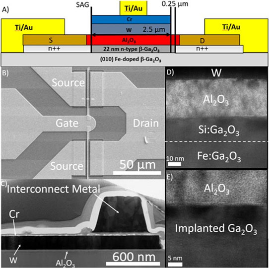
Figure 1: (a) Schematic of SAG β-Ga2O3 MOSFET, (b) top-down scanning electron microscope image of representative 2x50μm SAG MOSFET with dashed line indicating cross-sectioned region, (c) transmission electron microscope (TEM) image of gated region, and high-resolution TEM images of (d) W gate electrode, gate oxide and β-Ga2O3 substrate, and (e) gate oxide and implanted β-Ga2O3channel.
A silicon ion implant was made from the source side, giving a nominal gate-source distance (LGS) of 0μm, while the gate-drain distance (LGD) was 0.25μm due to shadowing effects. The Al2O3 gate dielectric layer also acted as an implant cap. The target doping of the implant region was 1x10²⁰/cm3.
Rapid thermal annealing at 900°C for 120s activated the silicon doping. High-resolution transmission electron microscopy (HR-TEM) studies of the final MOSFET showed no apparent damage to the interface between the W gate electrode and gate dielectric layer from the high-temperature annealing. There was also no sign of polycrystalline domains forming.
The device was completed with removal of Al2O3 from the source-drain regions with reactive-ion etch and the application of ohmic source-drain electrodes consisting of titanium/aluminium/nickel/gold (Ti/Al/Ni/Au) annealed at 470°C for 1 minute in nitrogen.
The devices were then electrically isolated from each other using plasma and reactive-ion etch. Interconnection for testing purposes consisted of Ti/Au metalization.
The researchers used Van der Pauw structures to extract a 4.96x10¹²/cm2 carrier sheet density and a 48.4cm2/V-s mobility. The sheet resistance was 2.6x10⁴Ω/square in the channel and 2.0x10³Ω/square in the implanted regions. The contact resistance was 1.5Ω-mm.
Electrical characterization of a 2.5μm gate-length device had a peak transconductance of 35mS/mm with 10V drain bias. The maximum drain current reached 140mA/mm. The on/off current ratio was 108, indicating good pinch-off. The subthreshold swing was 121mV/decade, described by the researchers as “excellent”. The on-resistance at small drain bias was 30Ω-mm with the gate at 4V.
Using a model based on the results, the researchers project that a 0.5μm gate device could achieve 0.6mS/mm transconductance, 350mA/mm drain current, and 17Ω-mm on-resistance. This performance would require suitable thermal management or pulsed operation to avoid self-heating.
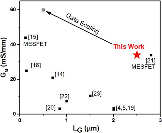
Figure 2: Peak transconductance (GM) versus gate length (LG) benchmarking of β-Ga2O3 FETs from this work (red), historical (black) and projection applying this process with sub-μm gate scaling (gray).
The team compared their work with that of others (Figure 2), commenting: “With the exception of vertically scaled delta-doped β-Ga2O3 MESFETs, the GM results are state-of-the-art and achieved with a large gate length.”
https://doi.org/10.7567/1882-0786/ab4d1c
The author Mike Cooke is a freelance technology journalist who has worked in the semiconductor and advanced technology sectors since 1997.


