


- News
2 August 2019
Electrically driven germanium-tin vertical-cavity surface emitter
Researchers in Taiwan and the USA claim the first electrically injected germanium-tin alloy (GeSn) vertical-cavity surface emitter on a silicon-on-insulator (SOI) platform [Bo-Jun Huang et al, ACS Photonics, published online 12 June 2019]. It is hoped that combining elements from group-IV of the Periodic Table will lead to easier integration with mainstream complementary metal-oxide-semiconductor (CMOS) silicon integrated electronics.
The team from Taiwan’s National Chung Cheng University, University of Massachusetts−Boston in the USA, and National Taiwan University comments: “Our demonstration paves the way toward the realization of room-temperature, electrically injected GeSn lasers to open up new avenues for functional scalable electronic-photonic integrated circuits.”
The problem is that the direct-bandgap transitions needed to produce photons are difficult to arrange in group-IV semiconductors. Generally, the lowest points of the conduction band are away from the symmetric central Γ point with zero quasi-momentum. However, progress has been made in the GeSn system in reducing the difference between the Γ point and the L-direction valleys, using strain and doping effects.
In the reported work, the researchers added electroluminescent enhancement from a vertical-cavity structure to give better optical confinement with suppressed radiation loss. Eventually it is hoped that vertical-cavity surface-emitting lasers (VCSELs) could be possible. Such devices would power SOI photonic systems targeted at applications such as fiber-optic telecommunication, light-detection & ranging (LiDAR), and chip-scale optical interconnection. The emission wavelengths fell mainly in the range 1600-2200nm, falling in the short-wavelength infrared (1400-3000nm).
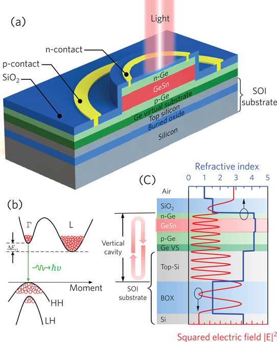
Figure 1: Three-dimensional schematic diagram of GeSn p−i−n heterodiode vertical-cavity surface emitter on SOI substrate (not to scale). (b) Schematic band diagram of Ge0.969Sn0.031 active layer. (c) Refractive-index profile and field pattern |E|2 of device simulated by finite-element method (FEM).
The LED structure was based on a double-barrier heterostructure design (Figure 1). The active GeSn layer was compressively strained to give a direct transition between the conduction and heavy-hole bands. The barriers were constituted from the 400nm p-type and 180nm n-type Ge contact layers.
Light was trapped between the buried oxide of the silicon-on-insulator substrate and silicon dioxide deposited during device fabrication. The trapping was based on reflection due to the low ~1.45 refractive index of the silicon dioxide and the high ~4.2 value for the Ge/GeSn layers. The reflection thus created a Fabry-Perot vertical cavity, enhancing light extraction.
The epitaxial material for the device came from low-temperature solid-source molecular beam epitaxy (SS-MBE). The 170nm Ge ‘virtual substrate’ layer transitioned from the SOI substrate to a strain-relaxed state according to inspection of the interfaces by cross-sectional transmission electron microscopy.
Secondary-ion mass spectroscopy (SIMS) and x-rays analyses gave a 3.1% Sn fraction and 0.454% compressive strain in the 440nm pseudomorphic GeSn active layer. The SOI substrate consisted of a 2.5μm top silicon layer on 1μm oxide. The p- and n-type Ge layers were doped with boron and antimony, respectively.
A comparison sample grown on silicon substrate had a 4.5% Sn fraction/0.659 compressive strain 420nm GeSn layer.
The researchers fabricated LEDs with a 200μm-diameter circular mesa and 420nm-thick SiO2 passivation. Ring-shaped ohmic contact pads were constructed from chromium/gold. The processing was CMOS compatible, according to the team.
The LEDs’ on/off current ratio was 200 between +1V and -1V. The electroluminescence (EL) of an LED grown on silicon consisted of a peak at 1900nm wavelength with 250nm full-width at half-maximum (FWHM). This corresponds to the direct transition energy of 650meV, according to the researchers. The reflectivity ripple of ~240nm free spectral range was attributed to interference between reflections from different layer interfaces.
The SOI-substrate LED emitted a series of peaks with FWHM around 66nm. The reflectivity free spectral range (FSR) was also shorter at around 110nm. The reflectivity dips matched the emission peaks.
The researchers comment: “Thus, comparing the EL and reflectivity spectra between the GeSn-on-SOI and GeSn-on-Si devices provides direct evidence for the longitudinal resonant cavity modes in the GeSn vertical cavity on SOI. In addition, despite the smaller Sn composition, the peak and integrated EL intensities of the GeSn-on-SOI devices are 6.31 and 3.7 times higher than those of the GeSn-on-Si device, highlighting the important EL enhancement owing to the cavity effect.”
The strongest peaks were around 1780nm and 1880nm, the relative importance of which varied with continuous-wave injection current (Figure 2). The researchers extracted quality factors for the cavity of 33 and 31 for the 1780nm and 1880nm wavelengths, respectively.
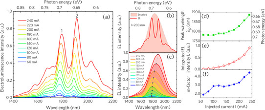
Figure 2: (a) Room-temperature EL spectra of GeSn-on-SOI device under different injected currents. (b) EL spectrum and mode envelopes at 200mA. (c) Mode envelopes at different injected currents. Peak wavelength of mode envelope (λp) indicated by gray dots. (d) Peak wavelength of mode envelope, (e) integrated EL intensity, and (f) m-factor as function of injected current.
The researchers see the bandgap narrowing due to Joule heating effects. The band edge thus moves out of the 1780nm region into the 1880nm cavity resonance corresponding to lower-energy photons. The Joule heating may also play a role in reducing the energy difference between the lower-energy indirect conduction-band valley (L) and the slightly higher direct valley (Γ). With a smaller energy difference, and higher temperature, more electrons can be excited into the Γ valley with potential for fast recombination into photons.
Although positive net optical gain was not achieved by the vertical-cavity structure, the gain for the longer-wavelength peak (~1880nm) did approach 0 as the injection current neared 200mA. The near zero gain “implies important absorption bleaching in the cavity toward achieving optical gain.” The gain then falls off due to further bandgap narrowing at high currents of ~240mA. Positive net optical gain would be needed for laser devices.
The researchers performed simulations that suggested that increased operating temperatures allied with low Sn content in the active region could create a direct bandgap. “These analyses suggest that our GeSn light emitter can perform better at elevated temperatures, thereby being suitable for silicon-integrated circuits in which the operation temperature can go up to 150°C (423K) due to the Joule heating effect”, the team writes.
According to the researchers, even without lasing capability, the vertical-cavity light emitter could find use in GHz-level direct modulation short-reach optical communications. The team sees prospects for room-temperature high-data-rate chip-to-chip or board-to-board free-space optical interconnects. The suggested link arrays would consist of vertical-cavity transmitters and receivers with or without lenses for optical beam formation.
GeSn Vertical-cavity surface emitter SOI substrate CMOS LEDs GeSn lasers
http://pubs.acs.org/doi/abs/10.1021/acsphotonics.8b01678
The author Mike Cooke is a freelance technology journalist who has worked in the semiconductor and advanced technology sectors since 1997.


