


- News
30 June 2017
High-quality nitrogen-polar gallium nitride vertical p-n diodes
Cornell University in the USA has developed vertical p-n diodes using nitrogen-polar c-plane (000-1) gallium nitride (GaN) growth [YongJin Cho et al, Appl. Phys. Lett., vol110, p253506, p2017]. The researchers report: “A very low dislocation density leads to a high reverse breakdown electric field of ~2.2MV/cm without fields plates — the highest reported for N-polar epitaxial structures.” They further claim that their devices are the highest-quality p-n diodes ever demonstrated on N-polar GaN in terms of reverse bias leakage.
The GaN crystal structure has strong charge polarization in the c-direction due to the ionic nature of the Ga-N chemical bond. The Cornell team suggests that growing material in the N-polar rather than more common Ga-polar form, reversing the polarization, could lead to new electronic and photonic device opportunities such as ultra-low-power tunneling transistors, buried barrier high-electron-mobility transistors, and interband tunnel junctions. Further polarization engineering is used to create two-dimensional electron gas (2DEG) transistor channel layers and can also be exploited to improve hole densities in p-type regions.
N-polar growth allows higher growth temperatures since the material is more robust against decomposition. However, bulk GaN substrates are usually prepared in Ga-polar form, and high-quality, low-dislocation, smooth N-polar GaN substrates have only recently become available.
The N-polar GaN (000-1) substrate for Cornell’s work was supplied by Ammono SA. The n+ doping in the substrate delivered an electron concentration around 1019/cm3. X-ray diffraction analysis suggested a dislocation density of 5x10⁴/cm2, much lower than the 109/cm2 typical of GaN material on alternative substrates. Root-mean-square roughness over a 10μmx10μm field was ~0.4nm, according to atomic force microscopy (AFM).
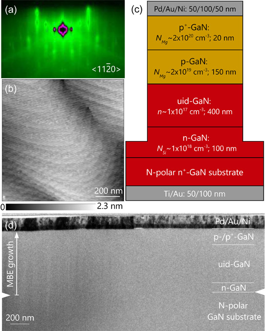
Figure 1: (a) In-situ reflection high-energy electron diffraction (RHEED) pattern showing (3x3) reconstruction characteristic of N-polar surface, and (b) AFM micrograph of MBE-grown N-polar GaN p-n diodes showing atomic steps. (c) Schematic layer structure and (d) cross-section transmission electron micrograph of fabricated vertical p-n diodes. Two white grooves on sides of image highlight interface between single-crystal bulk GaN substrate and MBE-grown epi-layers.
The p-n diodes (Figure 1) were grown using Ga-rich plasma-assisted molecular beam epitaxy (PAMBE) on a Veeco Gen Xplor machine. Excess Ga droplets were removed after growth by hydrochloric acid cleaning. Analysis of the diode material suggested that “the high structural perfection of the single-crystal GaN substrate was largely transferred to the MBE-overgrown p-n diodes,” according to the researchers. The diodes were fabricated with 600nm-high mesas for electrical isolation.
A 50μm-diameter device had a 3.5V turn-on voltage, close to that expected from the ~3.4eV bandgap of GaN. At 5V forward bias, the current density was 7.8kA/cm2, and the specific differential on-resistance was 0.1mΩ-cm2. The resistance was not corrected for the probe and therefore the actual value is smaller. Under reverse bias down to -6V, the leakage was less than 10-5A/cm2. The ±5V on/off current ratio was more than 109.
“This high performance proves high-quality N-polar GaN p-n diodes with a low dislocation density are now possible by MBE,” the researchers comment.
Electroluminescence was also observed with photon energy peaks at 3.13eV and 3.39eV with 5V forward bias and 1.5kA/cm2 current density. The 3.39eV was attributed to near-band-edge (NBE) emission. The 3.13eV emissions were assigned to conduction band-to-acceptor (CBA) transitions in p-GaN layers. The magnesium doping of p-GaN gives a hole binding energy around 0.25eV.
A very weak broad deep-level transition was also observed around 2.2eV. The team writes: “The presence of the NBE and CBA peaks, and the weak intensity of the broad band peak indicate a low density of deep point defects in the p-n diodes.”
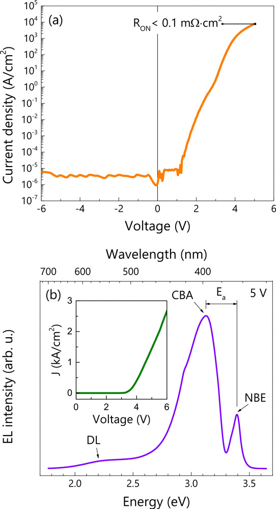
Figure 2: (a) Current density versus voltage characteristics of N-polar GaN single-crystal diodes in semilog scale showing high rectification ratio and low on-resistance. (b) Electroluminescence spectrum measured at 5V forward bias. Inset: linear-scale current density versus forward voltage.
Reverse-bias breakdown was studied using a 20μm-diameter diode. Abrupt breakdown occurred at -76V, just after the current leakage reached 10-1A/cm2 density. The researchers attribute the breakdown to trap-assisted avalanche effects as opposed to interband Zener tunneling.
Using capacitance-voltage measurements to estimate the electron concentration in the unintentionally doped (uid) GaN layer (9.6x10¹⁶/cm3), the researchers calculated that the peak electric field at breakdown was around 2.2MV/cm, occurring at the edge of the depletion region.
The team comments: “This breakdown electric field, lower than the best Ga-polar GaN p-n diodes of ~4MV/cm, nevertheless indicates the highest value for N-polar GaN p-n diodes and can be significantly improved by sculpting the electric field externally using field-plates as the Ga-polar counterparts. The full performance and true breakdown behavior of the diodes may be accessible by electrically isolating the device regions from edge sidewalls.”
N-polar GaN GaN p-n diodes MBE PAMBE Veeco
http://dx.doi.org/10.1063/1.4989581
The author Mike Cooke is a freelance technology journalist who has worked in the semiconductor and advanced technology sectors since 1997.


