


- News
23 March 2016
Exciton control in molbdenum disulfide
University of California at San Diego (UCSD) in the USA and the University of Manchester in the UK have been developing methods to control excitons in molybdenum disulfide (MoS2) [E. V. Calman et al, Appl. Phys. Lett., vol108, p101901, 2016].
The researchers hope that states such as Bose-Einstein condensates found in low-temperature gallium arsenide (GaAs) exciton structures could be realized at room temperature, giving access to resistance-free superfluid flow. Also, better control of excitons is considered to be a path to more efficient light emission.
The use of MoS2 should allow exciton states to be studied at room temperature and above. Gallium arsenide excitons have much smaller binding energies, and thus cannot survive temperatures above 100K.
MoS2 is a transition metal dichalcogenide (TMD) – a group of materials that can be separated into atomic-scale layers. Much present research is being carried out into the properties of MoS2 and other materials in this class, such as molybdenum diselenide, tungsten disulfide, and tungsten diselenide.
In addition, there are other materials that can be separated along weak van der Waals-type bonds such as graphene, black phosphorus, and hexagonal boron nitride.
It is hoped in future to develop electronic devices and mass-production methods that could lead to small low-cost technology based on atomic-scale layers of materials.
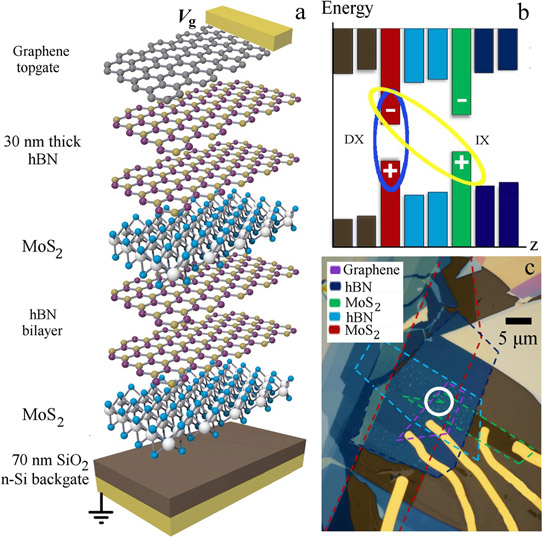
Figure 1. Coupled quantum well van der Waals heterostructure. Layer (a) and energy-band (b) diagrams. Ovals indicate direct (DX) and indirect (IX) excitons composed of electron and hole. (c) Microscope image showing layer pattern of device. Laser excitation target is indicated by circle.
The San Diego/Manchester test structure (Figure 1) was assembled from Scotch-tape mechanically exfoliated layers on a silicon dioxide layer on n-type silicon (n-Si) substrate. The Scotch-tape technique was developed at Manchester by one of the paper's authors, Andre Geim, in his Nobel-prize-winning research into graphene.
Coupled quantum wells of MoS2 monolayers were separated by a bilayer of hexagonal boron nitride (hBN). About 30nm of hBN was also used to give a dielectric cladding for the top graphene electrode. A 'gate' voltage (Vg) could be applied between the top electrode and n-Si substrate.
Photoluminescence was measured under various conditions using continuous wave (cw) laser excitation at three energies: 3.1eV, 2.3eV and 1.9eV.
Spectra were gathered at temperatures between 1.6K and 286K at 3.1eV excitation with 0.8mW power. Also, the laser power of a 2.3eV laser was varied between 0.5mW and 800mW. Circularly polarized light was used to probe spin relaxation. Pulsed excitation at 3.1eV was used for time-resolved spectra. The voltage across the structure was also varied between -20V and +40V.
The spectra showed three main peaks: two high-energy emissions separated by about 20meV, and a broader lower-energy state. The analysis arising from the various set ups suggested that the states were direct excitons – i.e. carrier bound states within the wells – rather than indirect states coupling carriers in different wells.
The high-energy peaks were considered to be from electron–hole bound states – A excitons, the 'A' referring the type of hole determined by spin-orbit coupling effects in the valence band. The binding energies of the two MoS2 A excitons were about 0.5eV, split by about 25meV. The splitting between A and B excitons in MoS2 is about 0.2eV.
The 0.5eV binding is much greater than the typical scale of fluctuations from thermal effects at room temperature of 26meV. Excitons in the usual compound semiconductors have binding energies of at most tens of milli-electron-volts (e.g. ~60meV in zinc oxide). Gallium arsenide has exciton binding energies of about 4.2meV.
The researchers suggest that the ~25meV splitting could be associated with the spin-dependence of the electron mass in the conduction band. The team writes: "The calculated 10% difference in the masses, 0.44 versus 0:49m0, of the conduction band spin states results in a 5% difference in the reduced electron–hole masses and, in turn, exciton binding energies. This leads to the energy splitting 25meV consistent with the experiment."
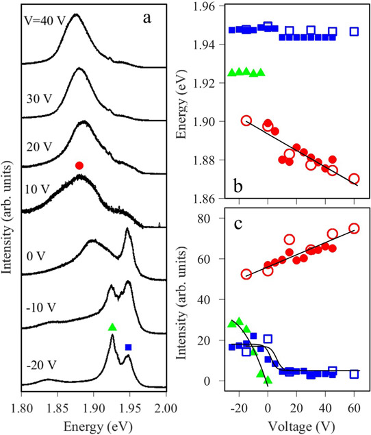
Figure 2. Gate voltage dependence. (a) Emission spectra at different Vg. Energy (b) and relative intensity (c) of emission lines marked in (a) versus Vg. Curves are guides to eye. Solid (open) symbols correspond to excitation energy 3.1eV (2.3eV) at 0:8mW power and 2K temperature.
The researchers associated the broad lower-energy state with charged excitons – trions – consisting of three carriers. The application of voltage across the structure enabled disentangling of the nature of the trions (Figure 2).
The researchers comment: "The main effect of the gate voltage in the direct regime is the control of the exciton and trion PL intensities: the high-energy exciton emission increased at the negative Vg, while the low-energy trion emission increased at the positive Vg. This behavior is attributed by the voltage-dependent electron concentration ne in the MoS2 layers."
Molbdenum disulfide Bose-Einstein condensates GaAs exciton structures
http://dx.doi.org/10.1063/1.4943204
The author Mike Cooke is a freelance technology journalist who has worked in the semiconductor and advanced technology sectors since 1997.


