

- News
16 April 2013
High power-gain cut-off frequency with high breakdown in GaN-on-Si HEMT
Institute of Electronic, Microelectronic and Nanotechnology (IEMN) in France has developed a gallium nitride (GaN) on silicon (Si) high-electron-mobility transistor (HEMT) with a power gain cut-off frequency of 220GHz and a three-terminal breakdown voltage above 100V [Farid Medjdoub et al, Appl. Phys. Express, vol6, p044001, 2013].
“For high-power applications, one of the most important figures of merit is the combination of the power gain with the three-terminal breakdown voltage (VBK) together with low dispersion,” according to the IEMN team. They add that their results give a record fmaxVBK product of 20.6THzV, “which is well beyond any previously reported data for GaN-on-Si devices and is comparable to the best GaN-on-SiC fmaxVBK product.” (Figure 1)
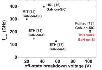 Figure 1: Benchmark of the power-gain cut-off frequency versus the off-state three-terminal breakdown voltage of GaN-on-SiC and GaN-on-Si devices.
Up to now, silicon carbide (SiC) has been the preferred substrate for high-current-density, high-speed GaN transistors capable of operating at high voltages and temperatures, due to the high thermal conductivity and the small lattice mismatch of SiC with GaN. However, SiC is very expensive, and much less costly silicon has been gaining favor with improving performance and maturity. In addition, the prospect is raised of combining GaN power devices monolithically with silicon CMOS logic.
The epitaxial material used for the IEMN transistors consisted of a double aluminium gallium nitride (AlGaN) heterostructure of AlN/GaN/AlGaN, produced on 4-inch-diameter highly resistive (111) silicon at metal-organic chemical vapor deposition (MOCVD) company EpiGaN (Figure 2). The delivered material included an in-situ silicon nitride (SiN) layer that both passivates the structure and prevents the relaxation of strain.
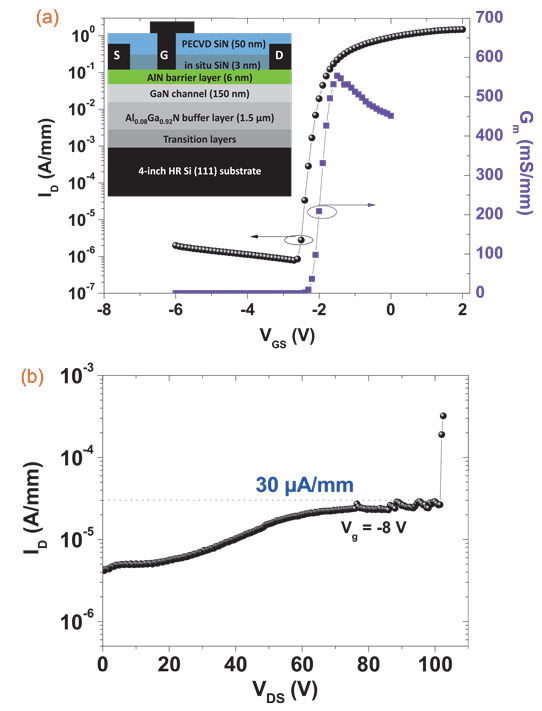
Figure 2: (a) Transfer characteristics of 0.12μm x 50μm AlN/GaN-on-Si DHFET at drain bias VDS = 6V. Inset: cross section of the fabricated device. (b) Off-state three-terminal breakdown voltage of 0.12x50μm AlN/GaN-on-Si DHFET.
The strain is used to create high carrier densities in the two-dimensional electron gas (2DEG) channel through the generation of polarization fields. Hall measurements give a carrier density of 2x10¹³/cm2 with a mobility of 1400cm2/V-s, resulting in a uniform sheet resistance of ~240Ω/square (+/-2.3%).
The ohmic source-drain contacts of titanium/aluminium/nickel/gold were formed directly on etched regions exposing the AlN layer. These contacts were rapidly annealed at 875°C. Device isolation was achieved with nitrogen implantation.
A further 50nm of SiN was applied using plasma-enhanced chemical vapor deposition (PECVD). A 120nm gate-length was defined using electron-beam lithography followed by sulfur hexafluoride (SF6) plasma etch down to the AlN. The etch process was designed to avoid plasma damage under the gate. The nickel/gold gate (with optimized field plate) was formed with additional electron-beam lithography and deposition.
Other dimensions of the device were 0.2μm gate-source and 0.3μm gate-drain spacing, and 50μm gate width.
The maximum current density with a +2V gate and 6V drain bias was 1.5A/mm (Figure 2a). The peak extrinsic transconductance was more than 550mS/mm. The off-state leakage was less than 2μA/mm.
The three-terminal breakdown voltage was more than 100V (Figure 2b). Below 100V drain bias, the drain leakage remained less than 30μA/mm.
Measurements with pulsed biasing of 500ns showed no threshold voltage shifts up to 30V drain bias. The researchers attribute this to “enhancement of the electron confinement in the 2DEG resulting from the use of the AlGaN back barrier”.
High-frequency testing was carried out up to 110GHz, giving a current gain cut-off (fT) of 75GHz and a power gain cut-off (fmax) of 220GHz at gate bias of -1.6V and drain bias of 20V. The researchers comment: “The high transconductance associated with the reduction of the short-channel effect by introducing a back barrier explains the outstanding power gain above 200GHz.”
The drain bias dependence of the cut-offs are that fmax increases to saturation at 20V, while fT decreases due to the impact of self-heating on transconductance.
The researchers believe that further performance improvement could be obtained from reduction of contact resistances and residual RF losses. In particular, the access resistances were relatively high and the residual RF loss appears to emanate from the interface between buffer and silicon substrate, which have a high lattice mismatch.
The researchers conclude: “These results show that GaN-on-Si devices have excellent potential for millimeter-wave applications, and will enable low-cost and next-generation highly integrated circuits.”
GaN-on-Si HEMT EpiGaN MOCVD PECVD
http://apex.jsap.jp/link?APEX/6/044001
The author Mike Cooke is a freelance technology journalist who has worked in the semiconductor and advanced technology sectors since 1997.
