- News
8 July 2011
Quaternary nitride HEMT with record cut-off frequency
University of Notre Dame and epiwafer supplier Kopin Corp of Taunton, MA, USA are claiming a record current-gain cut-off frequency (fT) of 220GHz for a nitride semiconductor high-electron-mobility transistor (HEMT) with quaternary indium aluminum gallium nitride (InAlGaN) barrier layer [Ronghua Wang et al, IEEE Electron Device Letters, published online 27 June 2011].
Nitride HEMTs normally use an AlGaN barrier, but recent work has suggested that lattice-matched InAlN with ~17% In can improve DC and radio frequency (RF) performance. However, the mobility of the electrons in the two-dimensional electron gas (2DEG) that forms the channel at the barrier/GaN buffer interface can be low. The 2DEG is used as the source of channel carriers in nitride HEMTs.
The problem of low mobility seems to stem from the tendency of the InN and AlN components of the InAlN alloy to separate (immiscibility) during crystal formation. This leads to increased interface roughness arising from microscopic variations in the strain field of the material. In turn, the interface roughness creates increased scattering of carriers and hence reduces mobility (~1600cm2/V-s for InAlN/AlN/GaN, as opposed to ~1800–1900cm2/V-s for AlN/GaN). Predictions suggest that InAlGaN has a narrower immiscibility gap than InAlN, and lattice-matched In0.16Al0.74Ga0.01N/AlN/GaN has achieved mobility of more than 1700cm2/V-s.
In addition to the depletion-mode (normally-on) HEMT that was demonstrated, the Notre Dame/Kopin researchers see possibilities for quaternary use in ultraviolet light-emitting diodes and enhancement-mode (normally-off) HEMTs, arising from the greater freedom to adjust the strain and bandgap energy. On the negative side, quaternary growth is more complicated and it is presumably less easy to control crystal quality.
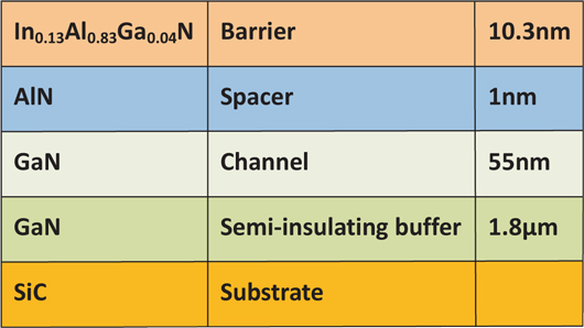
Figure 1: Schematic epitaxial structure, as determined using high-resolution x-ray diffraction and transmission electron microscopy, and secondary-ion mass spectroscopy.
Kopin grew the epitaxial structure (Figure 1) on a silicon carbide substrate using metal-organic chemical vapor deposition (MOCVD). The InAlGaN barrier was in tension in comparison to the GaN lattice structure. Mesa isolation was achieved using a chlorine-based reactive ion etch. Ohmic contacts consisted of silicon-titanium-aluminum-nickel-gold, annealed at 860°C in nitrogen. The contact resistance was measured through transmission-line method (TLM) structures at 0.36Ω-mm. Non-recessed rectangular gates consisted of nickel-gold. The physical dimensions of the HEMT were 1.6μm source–drain distance, with a source–gate distance of 300nm. The gate length was 66nm, and the width was 2μm x 50μm.
A dielectric-free passivation process was used, consisting of oxygen plasma treatment. The passivation reduced the sheet resistance from 227Ω/sq to 190Ω/sq, with an increase in carrier sheet concentration from 1.5x10¹³/cm2 to 1.8x10¹³/cm2. The passivation did decrease the mobility somewhat from 1900cm2/V-s to 1790cm2/V-s, attributed to enhanced scattering resulting from the higher carrier sheet concentration. “These mobilities are both among the highest reported, leading to the lowest sheet resistance in InN-containing HEMT structures.”
 The mobility in these quaternary InAlGaN structures was some 38% higher than that for InAlN devices created by the same group. The achievement is credited to reduced interface roughness and alloy scattering effects.
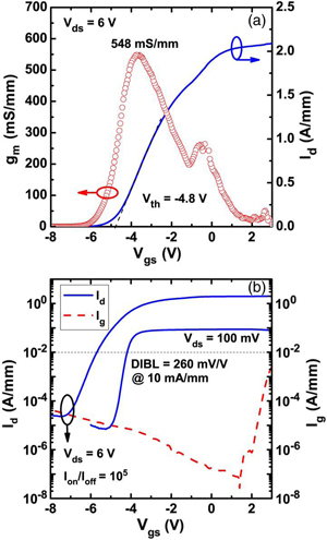
The maximum drain current with a 6V drain bias was 2.1A/mm (Figure 2a), measured at a gate potential of 3V. The threshold voltage was –4.8V. The maximum extrinsic transconductance was 548mS/mm, corresponding to an instrinsic value of 710mS/mm (i.e. subtracting the effect of source resistance). The researchers are investigating the reason for the small second peak in the transconductance curve shown in Figure 2a. A similar second peak has also been seen in InAlN/GaN HEMTs.
Figure 2: Transfer characteristics of the device measured drain voltages of 6V and 100mV (0.1V), in (a) linear scale and (b) semi-log scale.
The drain-induced barrier lowering (DIBL) of 260mV/V was determined by comparing the gate potentials needed to give a drain current of 10mA/mm with drain biases of 6V and 0.1V (i.e. 100mV). This is a high value, showing the presence of unwanted ‘strong’ short-channel effects. The on/off current ratio was ~105. The researchers comment: “To suppress the observed short-channel effects, use of back barriers and thinner top barriers is needed.”
Radio frequency measurements were performed in the range 250MHz–60GHz. The peak current gain cut-off frequency (fT) condition was achieved at 4.7V drain and –3.7V gate biases. The measured cut-off was 220GHz, with maximum oscillation frequency (fMAX) of 60GHz (153/54GHz, respectively, without de-embedding). The relatively low fMAX was blamed on the use of a resistive rectangular gate.
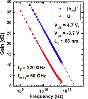 The researchers comment: “To the best of our knowledge, fT = 220GHz reported in this letter is the highest achieved in quaternary barrier GaN-based HEMTs to date and is also among the highest reported in all GaN-based HEMTs. Accordingly, a high fTxLg product of 14.5GHz-μm was achieved for a gate-length:barrier-thickness aspect ratio of 5.8.”
Kopin claims that it is “the world’s dominant provider of GaAs (gallium arsenide) heterojunction bipolar transistor (HBT) wafers with a dominant share of the worldwide merchant market”. It produces a variety of structures using AlGaAs, InGaP and even GaAsInN compound semiconductor material.
Figure 3: Current gain and unilateral gain of the device, showing fT/fMAX = 220/60GHz.
The Notre Dame/Kopin work was supported by US Defense Advanced Research Projects Agency (DARPA), US Air Force Office of Scientific Research, and US Air Force Research Laboratory/Missile Defense Agency.
University of Notre Dame Kopin HEMT InAlGaN MOCVD
The author Mike Cooke is a freelance technology journalist who has worked in the semiconductor and advanced technology sectors since 1997.