| Home | About Us | Contribute | Bookstore | Advertising | Subscribe for Free NOW! |
| News Archive | Features | Events | Recruitment | Directory |
News
6 October 2010
Georgia Tech uses patterned SiC templates to direct graphene growth
In the advance online edition of Nature Nanotechnology (3 October), Georgia Institute of Technology has reported a new ‘templated growth' technique that they have developed for fabricating nanometer-scale graphene devices, through work supported by the US National Science Foundation (NSF), the W.M. Keck Foundation, and the Nanoelectronics Research Initiative’s Institute for Nanoelectronics Discovery and Exploration (INDEX). The researchers say that the new method addresses what had been a significant obstacle to the use of this material in future generations of high-performance electronic devices.
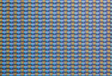 Picture: Graphene transistors.
Graphene (a one-atom-thick layer of graphitic carbon) has the highest known carrier mobility, giving it the potential to make radio-frequency electronic devices faster and smaller. However, the material's unique properties have led to difficulties in integrating it into such electronic devices. Conventional fabrication processes cannot readily be applied to produce graphene transistors because they often introduce significant defects into the monolayer of carbon lattices and severely degrade the device performance.
The new technique involves etching patterns into the silicon carbide (SiC) surfaces on which epitaxial graphene is grown. The patterns serve as templates directing the growth of graphene structures, allowing the formation of nanoribbons of specific widths without the use of electron beams or other destructive cutting techniques. The graphene nanoribbons that were produced have smooth edges that avoid electron-scattering problems.
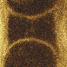 Picture: Graphene nanoribbon.
“Using this approach, we can make very narrow ribbons of interconnected graphene without the rough edges,” says professor Walt de Heer of Georgia Tech’s School of Physics. “Anything that can be done to make small structures without having to cut them is going to be useful to the development of graphene electronics because, if the edges are too rough, electrons passing through the ribbons scatter against the edges and reduce the desirable properties of graphene,” he adds.
The new technique has been used to fabricate an array of 10,000 top-gated graphene transistors on a 0.24cm2 chip (believed to be the largest density of graphene devices reported so far).
In creating their graphene nanostructures, De Heer and his team first use conventional microelectronics techniques to etch ‘steps’ — or contours — into an SiC wafer. They then heat the contoured wafer to about 1500ºC, which initiates melting that polishes any rough edges left by the etching process.
They then use established techniques for growing graphene from SiC by driving off the silicon atoms from the surface. Instead of producing a consistent layer of graphene one atom thick across the surface of the wafer, however, the researchers limit the heating time so that graphene grows only on the edges of the contours.
To do this, they take advantage of the fact that graphene grows more rapidly on certain facets of the SiC crystal than on others. The width of the resulting nanoribbons is proportional to the depth of the contour, providing a mechanism for precisely controlling the nanoribbons. To form complex graphene structures, multiple etching steps can be carried out to create a complex template, de Heer explained.
“By using the silicon carbide to provide the template, we can grow graphene in exactly the sizes and shapes that we want,” he says. “Cutting steps of various depths allows us to create graphene structures that are interconnected in the way we want them to be.”
In nanometer-scale graphene ribbons, quantum confinement makes the material behave as a semiconductor suitable for the creation of electronic devices. But in ribbons a micron or more wide, the material acts as a conductor. Controlling the depth of the SiC template allows the researchers to create these different structures simultaneously, using the same growth process.
“The same material can be either a conductor or a semiconductor depending on its shape,” notes de Heer, who is also a faculty member in Georgia Tech’s NSF-supported Materials Research Science and Engineering Center (MRSEC). “One of the major advantages of graphene electronics is to make the device leads and the semiconducting ribbons from the same material. That’s important to avoid electrical resistance that builds up at junctions between different materials,” he adds.
After formation of the nanoribbons — which can be as narrow as 40nm — the researchers apply a dielectric material and metal gate to construct field-effect transistors (FETs). While fabrication of high-quality transistors demonstrates graphene’s viability as an electronic material, de Heer sees them as only the first step in what could be done with the material. “When we manage to make devices well on the nanoscale, we can then move on to make much smaller and finer structures that will go beyond conventional transistors to open up the possibility for more sophisticated devices that use electrons more like light than particles,” he says. “If we can factor quantum mechanical features into electronics, that is going to open up a lot of new possibilities.”
De Heer and his team are now working to create smaller structures, and to integrate the graphene devices with silicon. The researchers are also working to improve the FETs with thinner dielectric materials.
Ultimately, graphene may be the basis for a generation of high-performance devices that will take advantage of the material's unique properties in applications where the higher cost can be justified. Silicon will continue to be used in applications that don’t require such high performance, de Heer says. “This is another step showing that our method of working with epitaxial graphene on silicon carbide is the right approach and the one that will probably be used for making graphene electronics,” he adds.
See related items:
UCLA sets record cut-off frequency of 300GHz for graphene transistors
![]() Search: SiC templates Graphene
Search: SiC templates Graphene
Visit: www.gatech.edu
For more: Latest issue of Semiconductor Today
![]() ©2010 Juno Publishing and Media Solutions Ltd. All rights reserved. Semiconductor Today and the editorial material contained within it and related media is the copyright of Juno Publishing and Media Solutions Ltd. Reproduction in whole or part without permission from Juno Publishing and Media Solutions Ltd is forbidden. In most cases, permission will be granted, if the author, magazine and publisher are acknowledged.
©2010 Juno Publishing and Media Solutions Ltd. All rights reserved. Semiconductor Today and the editorial material contained within it and related media is the copyright of Juno Publishing and Media Solutions Ltd. Reproduction in whole or part without permission from Juno Publishing and Media Solutions Ltd is forbidden. In most cases, permission will be granted, if the author, magazine and publisher are acknowledged.
Disclaimer: Material published within Semiconductor Today and related media does not necessarily reflect the views of the publisher or staff. Juno Publishing and Media Solutions Ltd and its staff accept no responsibility for opinions expressed, editorial errors and damage/injury to property or persons as a result of material published.
Semiconductor Today, Juno Publishing and Media Solutions Ltd, Suite no. 133, 20 Winchcombe Street, Cheltenham, GL52 2LY, UK
Web site by No Name No Slogan ![]()