| Home | About Us | Contribute | Bookstore | Advertising | Subscribe for Free NOW! |
| News Archive | Features | Events | Recruitment | Directory |
CMP PROCESSING
Learn more about R&D chemical mechanical polishing by requesting our FREE informational CD.

| FREE subscription |
| Subscribe for free to receive each issue of Semiconductor Today magazine and weekly news brief. |
News
4 January 2008
JPSA awarded LED wafer scribing patent
J. P. Sercel Associates Inc (JPSA) of Manchester, NH, USA, a designer, supplier, and systems integrator of laser-based materials processing workstations, has been awarded a patent, applicable in Korea, for its front-side laser scribing technique for sapphire LED wafers.
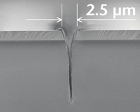 The technique involves the use of a unique laser energy distribution method that allows extremely narrow kerf widths (2.5 microns wide), resulting in faster processing and higher yields. Narrower kerfs also yield more die per wafer.
JPSA developed the LED sapphire wafer dicing capability with its IX-200 Chromadice DPSS UV laser wafer singulation system. “Our Chromadice system, using this patented process, can process fifteen 2-inch wafers per hour,” says president Jeffrey P. Sercel. “That represents a dramatic increase in throughput compared to diamond scribing and conventional laser techniques,” he claims.
The IX-200 ChromaDiceT DPSS is also suitable for wafer trimming and scribing applications. Its UV diode-pumped solid-state (DPSS) laser system delivers high-speed wafer dicing and cutting with typical yields of greater than 99% at less than $2 per wafer. The process is tolerant of wafer warp and bow and suitable for all wafer types, JPSA says. The system is also available in an excimer laser version for via drilling, micromachining, thin-film patterning and other packaging applications, including LED liftoff.
See related items:
JPSA recruits application and process engineering specialist
JPSA appoints Larry Roberts as director of engineering
Search: JPSA Sapphire LED wafers
Visit: www.jpsalaser.com
![]()
![]() ©2008 Juno Publishing and Media Solutions Ltd. All rights reserved. Semiconductor Today and the editorial material contained within it and related media is the copyright of Juno Publishing and Media Solutions Ltd. Reproduction in whole or part without permission from Juno Publishing and Media Solutions Ltd is forbidden. In most cases, permission will be granted, if the author, magazine and publisher are acknowledged.
©2008 Juno Publishing and Media Solutions Ltd. All rights reserved. Semiconductor Today and the editorial material contained within it and related media is the copyright of Juno Publishing and Media Solutions Ltd. Reproduction in whole or part without permission from Juno Publishing and Media Solutions Ltd is forbidden. In most cases, permission will be granted, if the author, magazine and publisher are acknowledged.
Disclaimer: Material published within Semiconductor Today and related media does not necessarily reflect the views of the publisher or staff. Juno Publishing and Media Solutions Ltd and its staff accept no responsibility for opinions expressed, editorial errors and damage/injury to property or persons as a result of material published.
Semiconductor Today, Juno Publishing and Media Solutions Ltd, Suite no. 133, 20 Winchcombe Street, Cheltenham, GL52 2LY, UK
Web site by No Name No Slogan ![]()