| Home | About Us | Contact Us | Contribute | Advertising | Subscribe for Free NOW! |
| News Archive | Features | Events | Recruitment | Directory |
Editor:
Mark Telford (Email)Tel:+44 (0)1869 811577
Cell:+44 (0)7963 085605
Fax:+44 (0)1242 2911482
Commercial Director /
Assistant Editor:
Darren Cummings (Email) Cell:+44 (0)7990 623395
Fax:+44 (0)1242 2911482
Advertising Manager
Jon Craxford (Email)Tel:+44 (0)207 1939749
Cell:+44 (0)7989 558168
Fax:+44 (0)1242 2911482
Features
July 2006
Nitride substrates bridging the gap
Dr Mike Cooke summarizes the relative merits of the various substrate types for nitride-based devices, as well as the latest commercial developments.
Since Shuji Nakamura invented and developed the first commercial processes for blue-green light emitting devices based on gallium nitride (Figure 1a), nitride semiconductor technology has become an important focus for research, development and commercial products. Renewed interest has been sparked by the prospect of GaN high-electron-mobility field-effect transistors (HEMTs) being used in wireless base-stations to provide RF power amplification up to 40 GHz (Figure 1b) [1]. This application is dependent on increasing the reliability of the devices, partly through reducing the defect density in the GaN substrate layer. Defects are even more effective at killing high-stress devices such as continuous-wave operation laser diodes. Other possible future applications of nitride technology include power switching, ultraviolet detection and bio-chemical sensing.
GaN’s commercial success has been enabled by GaN being grown hetero-epitaxially on other materials such as silicon carbide (SiC) and sapphire (Al 2 O 3 ). In recent years, there have been attempts to grow single-crystal GaN (Table 1) to provide a substrate for homo-epitaxial GaN. Other companies have aimed to produce epitaxial GaN layers more cost effectively using substrates including silicon (Nitronex, Cree, PicoGiga), aluminium nitride (Crystal IS, Fox Group), or zinc oxide (Cermet).
Figure 1 show schematic diagrams of GaN-based light-emitting diodes (LEDs) and field-effect transistors (FETs), where the GaN epilayer on these wafers is followed by a series of layers consisting of alloys of Group III elements (Al, Ga, In) with nitrogen. Ternary (e.g. AlGaN) and quaternary (e.g. InAlGaN) combinations can be used to engineer the band structures and lattice properties required. Although a linear interpolation between the properties of the binary compounds (Table 2) can give a first approximation, it is often necessary to include higher-order effects.
Sapphire
At first sight, sapphire does not provide the most promising surface on which to grow GaN. The lattice mismatch is about 15% (Table 3) and the coefficients of thermal expansion differ, which is a problem as the GaN layers are fabricated, and often designed to run, at high temperature. GaN layers on sapphire that are stable during growth at 1000°C can crack on cooling to room temperature. Further, thermal stresses can cause propagation of defects up from the GaN layer either before or during operation. 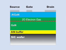
Despite these problems, in the late 1980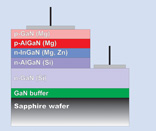 s, Japanese researchers pioneered viable techniques to grow GaN on sapphire by MOCVD, triggering the explosion in commercial blue–green lightemitting devices of the 1990s. First, researchers from Nagoya University and Matsushita Electric Industries produced substrates with an AlN buffer layer between the sapphire and GaN materials [4]. Then Shuji Nakamura at Nichia used a AlGaN buffer [5].
Typical MOCVD steps for producing GaN on sapphire include a pre-treatment at around 1000°C (to nitride the sapphire surface, typically using ammonia, NH3), production of a nucleation layer at about 600°C, then reheating to a growth temperature of 1000°C. The resulting wafer consists of a highly dislocated buffer layer near the sapphire substrate that gradually becomes more crystalline (Figure 2a).
To improve the final GaN layer, various techniques have since been developed, such as lateral epitaxial overgrowth (LEO), where GaN is grown around a SiO2 mask that blocks the threading dislocation defects propagating upwards from the buffer region (Figure 2b). The method can lead to crystallographic ‘tilt’ between regions that have overgrown the mask and coalesced.
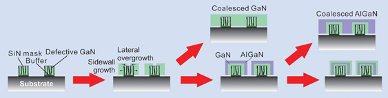
Alternatively, in ‘pendeo-epitaxy’ (Figure 3), GaN crystal growth proceeds from the sidewalls of columns of GaN seed layers etched onto the substrate, and then overgrows the SiN mask on top of the column. Further growth options are available, such as continuous GaN or AlGaN films. These techniques can be used independently of the initial substrate material (e.g. on SiC substrates). North Carolina State University developed two separate ‘pendeo’ patent portfolios: one, for SiC substrates, was sold to Cree under an exclusive agreement; the other, for GaN/sapphire and GaN/Si, was used to found Nitronex.
Silicon carbide
Compared to sapphire as a GaN substrate, 4H and 6H polytypes of silicon carbide have much smaller lattice mismatches of 3-4%. Also, at room temperature, SiC’s thermal conductivity is ten times that of sapphire (a thermal insulator, and unusable for high-power-density GaN devices). Good thermal conductivity is particularly important for devices operating at over 200°C, such as RF power transistors and high-power lighting devices, which need an effective dissipation path to heat sinks and other thermal control fixtures.
The main drawback is that good-quality, large-diameter SiC is very difficult to produce and is hence expensive. The Czochralski method for producing high-quality silicon crystal does not work, since there is no SiC liquid phase at atmospheric pressure (and likewise for AlN). In fact, solid SiC only melts at about 2800°C and at a pressure greater than 35 atmospheres. Bulk SiC crystals are sublimated directly from the gas phase. Careful process control is needed to avoid defects such as dislocations, the inclusion of different polytypes, and micropipes.
Much effort has been made to improve SiC crystal quality, especially since it is important for high-voltage devices in its own right: it is expected that SiC power transistors will be used for RF amplification of wireless base-station transmission signals, while GaN-based device reliability is improved.
In the past, the density of micropipes has been the dominant defect in limiting wafer cost-reduction and device size. However, micropipe density has since been reduced so that it is no longer dominant. Indeed, recently Intrinsic Semiconductor, for example, started commercial shipments of its ZMP (zero-micropipe) SiC wafers (targeted at reducing cost), as well as 100mm (4-inch) SiC wafers.
GaN
In addition to the established substrates, there is a wide range of as-yet unrealised possibilities. Pure GaN substrates would avoid all the problems of lattice matching and thermal expansion, although its thermal conductivity (half that of SiC) is a slight drawback.
But, again, liquid-phase growth is not possible, as the N atom has a tendency to dissociate at about 1600°C, while the GaN melt temperature is about 2500°C. Despite this, many groups and companies have worked to produce pure GaN wafers via other processes. In hydride vapour phase epitaxy (HPVE), gallium and hydrochloric acid are made to react, creating volatile gallium chloride. The vapour is then transported to the crystal growth zone to react with an ammonia layer on the growing GaN crystal. Growth rates of hundreds of microns an hour can be achieved. Alternatively, GaN can be grown as a thick layer on a sapphire or SiC template, which is then removed, leaving a pure GaN wafer. Hitachi Cable has used a perforated titanium nitride film between the GaN and the template to ease separation.
Sumitomo Electric Industries (SEI) has a process where dislocations are reduced by forming inversepyramidal pits on the surface of the crystal (Dislocation Elimination by Epitaxial growth with inverse-pyramidal Pits/DEEP). It has also developed a technique that controls the area where dislocations are concentrated to form larger low-dislocation areas. SEI claims to be able to produce 500 μm-diameter areas with dislocation densities of 10 4 –10 5 cm -2 on a 50mm-diameter GaN wafer. Its original target for these techniques was the production of lasers for Blu-ray optical disks, shipping samples in 2002.
Silicon
Since the GaN-on-sapphire lattice mismatch has not stopped production of devices, one may wonder if the same is not possible with silicon. Research on GaN/Si was diverted by Nakamura’s success with sapphire substrates, but more recently companies have begun producing GaN/Si substrates for commercialization.
The GaN/Si lattice mismatch is about 18%, but its thermal conductivity is about four times that of sapphire (40% that of SiC). A further attraction is the availability of larger and much lower-cost substrates from the mainstream silicon industry. Among the buffer layers used to bridge the lattice mismatch are GaAs, AlAs, ZnO, LiGaO 2 (lithium gallate, or LGO for short), SiO 2 , Si 3 N 4 , sputtered AlN, low-temparture GaN (LT-GaN), LT-AlN, and deposited and converted SiC. Nitronex uses a proprietary recipe of transition layers in its SIGANTIC GaN/Si product. It can also use its trademarked PENDEO process to improve the GaN crystal quality, but has found this unnecessary for its most recent products.
SOITEC’s Picogiga International compound semiconductor material division in Europe has prod uced thin layers of single-crystal GaN on 150mm (111) Si wafers, also using a proprietary buffer layer. Picogiga uses MBE reactors, traditionally research tools with much slower growth rates than MOCVD, but available in recent years with production-scale throughputs: Picogiga claims a capacity of 70,000 100mm-equivalent epiwafers per year on 10 MBE tools from Riber and Veeco. In 2005, PicoGiga announced a joint development program with Veeco on the industrial-scale use of MBE in producing GaN/Si, targeting the first industrial MBE reactor for the process, based on Veeco’s GEN200 system, which can handle wafers up to 150mm.
SOITEC also hopes to apply its wafer bonding and SmartCut hydrogen implant technology used in its commercial silicon-on-insulator wafer production process to provide GaN substrates with improved thermal performance based on polycrystalline SiC (pSiC). Initially, a thin layer of (111) Si will be applied to the pSiC before the epitaxial growth of GaN, but the eventual aim is to put a pure GaN layer on the pSiC, from which epitaxial GaN can be grown.
Diamond
To address the problems of heat build-up associated with high-power and high-speed transistors, this February, the first GaN-on-diamond wafer was launched, developed over the last three years by Group4 Labs, founded in Menlo Park, CA, USA in 2003. In its 10mm x 10mm square Xero Wafer (available at $450 per unit, either freestanding or on a disposable silicon wafer mount), the atomically smooth, epi-ready GaN layer lies less than 0.5nm away from a 25μm-thick substrate of CVD-deposited polycrystalline diamond, which has a thermal conductivity 3–30x that of conventional semiconductors. So, heat can be extracted very efficiently from the active layers, boosting the power density of a transistor array by at least 10x over GaN-on-SiC, claims Group4 Labs.
Aluminium nitride
Aluminium nitride has also attracted some interest as a substrate for nitride devices. Its lattice mismatch with GaN is about 2%, and its thermal conductivity is about 80% that of SiC.
One technique for producing bulk AlN crystal is sublimation-recondensation. Schowalter et al [7] of Crystal IS and the State University of New York (SUNY) comment that the basics of this growth process are “straightforward”. But a less sanguine view is taken by Liu et al [8], a group from Kansas State University, SUNY (again!), the UK’s University of Bristol and the USA’s Oak Ridge National Laboratory, who discuss the difficulty of the inherently reactive growth environment at 2100°C, and compare the suitability of materials such as tantalum carbide, niobium carbide, tungsten, graphite, and hot-pressed boron nitride for furnace fixtures. Crystal IS offers 50mm AlN substrates with a quoted dislocation level of less than 1000/cm2, but this is for the AlN substrate alone (without a GaN layer).
HexaTech claims a commercially viable process combining the benefits of physical vapour transport (PVT) growth and seeded growth for the reproducible production of AlN single crystals. Although no figures are given, it says that its seeded growth technique enables the fabrication of AlN boules of pre-defined crystallographic orientation, and of reproducible quality.
Other substrates
Other possible substrates for nitride devices have been considered in research, including MgO, MgAl 2 O 4 , LiAlO 2 , LiGaO 2 , ZnO, and NiAl. The best lattice matches are given by LiAlO 2 (0.2%), LiGaO 2 (1.4%) and ZnO (2.2%).
ZnO was proposed by Cermet, which aimed to produce substrates at a cost comparable to sapphire.
Cermet claims a patented technology for the bulk crystal growth of high-melting-point materials such as ZnO. It says that these systems have also been used to melt and solidify AlN, and that a process for GaN is “under development”.
The company sees opportunities for light-emitting device applications, since ZnO is conductive, allowing a bottom contact, unlike sapphire-based LEDs. But ZnO has some hurdles that must be overcome. Foremost is that atomic hydrogen and dissociated ammonia attack ZnO, and both are present in large concentrations during standard MOCVD growth of GaN or InGaN.
Cermet and Georgia Institute of Technology are developing alternative growth methods to produce phosphor-free solid-state visible light sources with funding from the US Department of Energy. The aim is to integrate large-area ZnO substrate and lattice-matched nitride epitaxy technologies to address substrate, epitaxy, and solid-state lighting device limitations in terms of defect densities in both the nitride emitters and the bulk substrates.
Applications
According to the recent report “2003-2009 Silicon Carbide Market Analysis” by France’s Yole Développement, 90% of SiC wafer production is dedicated to GaN-based blue/white LED production (Figure 4). However, SiC substrates are very costly, so this could dwindle if companies can find less expensive alternatives.
John Palmour, Cree’s executive vice president of Advanced Devices, believes that GaN-on-SiC is the best option for RF, at least at frequencies above 3GHz, because of the thermal conductivity advantage. GaN-on-Si could be useful at lower frequencies, where there is a trade-off between performance and cost. Above 3GHz or so, says Palmour, GaN/Si experiences microwave losses in the substrate (since there is no semi-insulating silicon), and the thermal conductivity is just one third that of SiC.
Last year, Nitronex announced pre-production samples of GaN transistors on its silicon substrate technology aimed at WiMAX broadband wireless networking. Its family of WiMAX power transistors initially consists of 10W and 50W devices supporting both the 2.5GHz and 3.5GHz segments. The 50W, 3.5GHz device is nearing the end of sampling. Chris Rauh, Vice President of Sales and Marketing, says that, with initial design-ins and early revenue already rolling in, Nitronex expected to complete full production qualification by early July. Nitronex also aims to introduce transistors supporting 5.8GHz operation in 2006.
Dr Edwin Piner, director of materials engineering, challenges the view that GaN/Si cannot handle more than 3GHz. Nitronex uses float-zone silicon, where a polysilicon rod is passed through an RF furnace, allowing a thin layer of the silicon to be re-melted. The impurities prefer to remain in the melt region and are swept along to the end. Commercially available floatzone silicon is close to “intrinsic”, with impurity levels of the order of 10 11 cm -3 , just short of the process’ supposed physical limit of 10 9 –10 10 cm -3 . Resistivities exceeding 10 5 Ωcm can be achieved, two orders of magnitude better than silicon’s usual 100–1,000Ωcm and comparable to Cree’s semi-insulating 4H SiC wafer. For high-power GaN HEMT production, care is still needed to ensure that subsequent GaN/Si processing does not allow Al and Ga impurities (p dopants!) to reach the silicon, particularly in the buffer region.
Others producing GaN-based HEMTs for this market include Cree, Fujitsu, NEC and RF Micro Devices. To compete with existing silicon lightly doped drain MOS (LDMOS) chips, the target price for reliable wireless devices is no more than $1 per Watt. Other possible options include SiC MESFETs and GaAs devices.
One application where free-standing GaN substrates would be most beneficial is for lasers, since homo-epitaxy always gives the lowest defect densities. Extending the unfeasibly short lifetimes of GaN-based laser diodes depends critically on defect reduction (Table 4).
Bulk AlN substrates could prove useful for LEDs emitting in the deep-ultraviolet (DUV) region of the spectrum (less than 300nm) due to its much reduced light absorption compared with other options. This is because absorption in AlN is much suppressed below its bandgap energy of 6.2eV, which corresponds to a photon wavelength of 200nm. Applications for DUV LEDs include biological agent detection, non-line-ofsight (NLOS) covert communications, water purification, the curing of polymers and other chemicals, and in decontamination equipment. The first two of these applications explain the interest of the US Defense Advanced Research Projects Agency (DARPA), which, among others, funds research in the area.
Indeed, in May, a 210nm UV PIN LED grown homoepitaxially on an AlN substrate was reported in Nature by Japan’s NTT Basic Research Laboratories after achieving controllable n-type doping in lowdefect- density AlN. Such AlN-based devices will be explored more in future issues of Semiconductor Today in the context of AlGaN blue lasers.
References
[1] M. Cooke, III-Vs Review , December/January 2005/2006, p. 40 and February–April 2006.
[2] Many material properties can be found at: www.ioffe.rssi.ru/SVA/NSM/Semicond/ www.onr.navy.mil/sci_tech/31/312/ncsr/
[3] www.ioffe.rssi.ru/SVA/NSM/Semicond/InN/dvdv.html
[4] H. Amano et al , App. Phys. Lett . (1986) Vol.48, pp.353–5 US Patent 4,855,249, Akasaki et al , (1989)
[5] S. Nakamura, Jpn. J. Appl. Phys . (1991) Vol.30, pp.L1705–7 US Patent 5,290,393, Nakamura (1994). US Patent 5,433,169, Nakamura (1995)
[6] K.J. Gehrke et al , MRS Internet J. Semicond. Res . (1999) 4S1 , G3.2
[7] L.J. Schowalter et al , physica status solidi (2003) Vol. 0, No. 7, pp.1997–2000
[8] B. Liu et al , MRSInternet J. Nitride Semicond. Res . (2004) 9 , 6
[9] Y. Taniyasu et al , Nature ( 2006) 441 , 299
![]() ©2006 Juno Publishing and Media Solutions Ltd. All rights reserved. Semiconductor Today and the editorial material contained within it and related media is the copyright of Juno Publishing and Media Solutions Ltd. Reproduction in whole or part without permission from Juno Publishing and Media Solutions Ltd is forbidden. In most cases, permission will be granted, if the author, magazine and publisher are acknowledged.
©2006 Juno Publishing and Media Solutions Ltd. All rights reserved. Semiconductor Today and the editorial material contained within it and related media is the copyright of Juno Publishing and Media Solutions Ltd. Reproduction in whole or part without permission from Juno Publishing and Media Solutions Ltd is forbidden. In most cases, permission will be granted, if the author, magazine and publisher are acknowledged.
Disclaimer: Material published within Semiconductor Today and related media does not necessarily reflect the views of the publisher or staff. Juno Publishing and Media Solutions Ltd and its staff accept no responsibility for opinions expressed, editorial errors and damage/injury to property or persons as a result of material published.
Semiconductor Today, Juno Publishing and Media Solutions Ltd, Suite no. 133, 20 Winchcombe Street, Cheltenham, GL52 2LY, UK
Web site by No Name No Slogan ![]()