
| Home | About Us | Contribute | Bookstore | Advertising | Subscribe for Free NOW! |
| News Archive | Features | Events | Recruitment | Directory |
CMP PROCESSING
Learn more about R&D chemical mechanical polishing by requesting our FREE informational CD.

| FREE subscription |
| Subscribe for free to receive each issue of Semiconductor Today magazine and weekly news brief. |
News
10 October 2007
CrystalQ and Aixtron develop 6-inch GaN-on-sapphire wafer
Deposition equipment maker Aixtron AG of Aachen, Germany and sapphire wafer maker CrystalQ BV of Stadskanaal, The Netherlands have presented initial test results for a 6-inch (150mm) c-plane GaN-on-sapphire wafer. The development is a result of a joint R&D project started in mid-2005 within the framework of a European Union EUREKA collaboration.
Currently, the industry-standard wafer size is 2 inches, and a limited group of high-end LED makers have switched to processing 3- or 4-inch wafers. The feasibility of higher throughput requires scale-up of existing technologies to 6-inch wafers, says CrystalQ, for which fabrication technology for 6-inch c-plane sapphire wafers needs to be developed that ensures identical layer deposition results as for standard 2- and 4-inch diameters (e.g. high yield for LED chip manufacturing). However, Aixtron has developed a flexible AIX 2800G4 HT mass-production MOCVD deposition system that, as well as handling 2-inch wafers, can handle 6x6-inch sapphire wafers while ensuring optimum uniformity of epitaxial layer growth. "Together with partners, we are continuously developing the equipment to
reduce production cost," says Aixtron's director of marketing Rainer
Beccard.
For the same purpose, CrystalQ has enhanced its proprietary chemical mechanical polishing (CMP) process, with its tool design resulting in controllability of the roughness and flatness parameters of 6-inch c-plane sapphire substrates, the firm says. Effort has made to reduce the edge-exclusion zone in order to optimize the number of LED chips per wafer. As a result, the standard deviation of the wavelength on the photoluminescence map of the substrate was 2.48nm (0.55%) without edge exclusion.
 CrystalQ adds that the joint development project has also resulted in the implementation of a reclaim process for the reuse of 6-inch sapphire wafers, reducing operational costs for white LED makers.
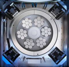
Picture: Shows the AIX2800G4 configured for 42 x 2" wafers, but capable of 6 x 6".
Search: Gallium nitride GaN-on-sapphire Sapphire wafers
Visit: www.crystalq.nl
Visit: www.aixtron.com
![]() ©2007 Juno Publishing and Media Solutions Ltd. All rights reserved. Semiconductor Today and the editorial material contained within it and related media is the copyright of Juno Publishing and Media Solutions Ltd. Reproduction in whole or part without permission from Juno Publishing and Media Solutions Ltd is forbidden. In most cases, permission will be granted, if the author, magazine and publisher are acknowledged.
©2007 Juno Publishing and Media Solutions Ltd. All rights reserved. Semiconductor Today and the editorial material contained within it and related media is the copyright of Juno Publishing and Media Solutions Ltd. Reproduction in whole or part without permission from Juno Publishing and Media Solutions Ltd is forbidden. In most cases, permission will be granted, if the author, magazine and publisher are acknowledged.
Disclaimer: Material published within Semiconductor Today and related media does not necessarily reflect the views of the publisher or staff. Juno Publishing and Media Solutions Ltd and its staff accept no responsibility for opinions expressed, editorial errors and damage/injury to property or persons as a result of material published.
Semiconductor Today, Juno Publishing and Media Solutions Ltd, Suite no. 133, 20 Winchcombe Street, Cheltenham, GL52 2LY, UK
Web site by No Name No Slogan ![]()