
| Home | About Us | Contribute | Bookstore | Advertising | Subscribe for Free NOW! |
| News Archive | Features | Events | Recruitment | Directory |
CMP PROCESSING
Learn more about R&D chemical mechanical polishing by requesting our FREE informational CD.

| FREE subscription |
| Subscribe for free to receive each issue of Semiconductor Today magazine and weekly news brief. |
News
14 November 2007
Micromem's Hall cross sensor meets expectations; on schedule for functioning MRAM by year end
Fabless GaAs memory firm Micromem Technologies Inc of Toronto, Canada says that several Hall cross sensor devices have now been manufactured at various features sizes as it drives the overall cell feature size of its magnetic random access memory (MRAM) technology to the limits of its GaAs wafer foundry partner, Global Communication Semiconductors Inc (GCS) of Torrance, CA, USA.
A Hall cross sensor device was manufactured and tested that functions precisely in accordance with the University of Toronto sensitivity model, notably:
- the sensor demonstrated excellent linearity;
- the magnetic field reversal yields symmetrical V(Hall) within expected tolerances;
- I(bias) reversal yields symmetrical V(Hall) within expected tolerances.
“What this means for the foundry phase is that Micromem’s Hall cross sensor device is extremely accurate, repeatable and linear - all necessary features for a memory design. The results have exceeded our expectations,” says project director Steve Van Fleet. “As a result of the tremendous performance, we plan to also use the Hall cross sensor devices as credible on-wafer sensors to evaluate our optimization efforts for the placement of the magnetic yoke structures.”
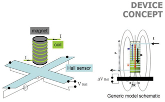
The Hall sensor forms an integral component of Micromem’s MRAM design, as it is used to measure the external field of a magnet whose magnetization can be reversed by generating a current in a coil.
“Having exceeded the test requirements on the Hall cross sensor device, we have authorized the foundry to accelerate their efforts on complete MRAM cell manufacturing,” says Van Fleet . He promises an additional update on actual memory cell testing prior to 25 December.
“As a result of this positive test data, we have defined the first MRAM array sizes that we are targeting,” says Van Fleet. These have been defined in concert with interested end-users. Initial target MRAM array sizes are 40 bits, 256 bits, 512 bits and 1024 bits. “In addition to these high-speed memory size requirements, we have been requested to design a 16K bit memory array of low-speed embedded memory,” he adds. “This will be used for identification purposes only, where radiation hardening is the key parameter and typically high-speed memory read-write time is not critical.”
See related items:
Micromem’s GaAs MRAM device processed at GCS
Micromem engages GCS as foundry for MEMS
Visit:
![]()
![]() ©2007 Juno Publishing and Media Solutions Ltd. All rights reserved. Semiconductor Today and the editorial material contained within it and related media is the copyright of Juno Publishing and Media Solutions Ltd. Reproduction in whole or part without permission from Juno Publishing and Media Solutions Ltd is forbidden. In most cases, permission will be granted, if the author, magazine and publisher are acknowledged.
©2007 Juno Publishing and Media Solutions Ltd. All rights reserved. Semiconductor Today and the editorial material contained within it and related media is the copyright of Juno Publishing and Media Solutions Ltd. Reproduction in whole or part without permission from Juno Publishing and Media Solutions Ltd is forbidden. In most cases, permission will be granted, if the author, magazine and publisher are acknowledged.
Disclaimer: Material published within Semiconductor Today and related media does not necessarily reflect the views of the publisher or staff. Juno Publishing and Media Solutions Ltd and its staff accept no responsibility for opinions expressed, editorial errors and damage/injury to property or persons as a result of material published.
Semiconductor Today, Juno Publishing and Media Solutions Ltd, Suite no. 133, 20 Winchcombe Street, Cheltenham, GL52 2LY, UK
Web site by No Name No Slogan ![]()