


News: LEDs
20 July 2022
UIUC demos cubic GaN on large-area U-grooved silicon (100) dies
Gallium nitride (GaN) and its alloys (i.e. III-nitride semiconductors) are the backbones of solid-state lighting, and next-generation RF and power electronics. Most R&D in this material system is currently focused on its conventional, hexagonal (i.e. wurtzite) phase.
However, its cubic (i.e. zincblende) phase has more inherent advantages. These include: no polarization in the <100> growth direction, smaller bandgap, smaller electron-heavy hole effective masses, less Auger loss, larger optical gain, shorter radiative recombination lifetime, lower p-doping activation energy, higher hole mobility, and larger conduction-band offset.
Cubic III-nitride semiconductors might thus enable next-generation devices such as efficiency-droop-free III-nitride visible light-emitting diodes (LEDs) and as-grown, normally-off aluminium gallium nitride/gallium nitride (AlGaN/GaN) power transistors. However, the synthesis of cubic GaN has not been an easy task due to its metastability.
In ‘Structural and Optical Properties of Cubic GaN on U-grooved Si(100)’ (J.Lee, Y. C.Chiu, M.A.Johar and C.Bayram, Appl. Phys. Lett. 121, 032101 (2022)), a team at the University of Illinois at Urbana-Champaign (UIUC) team has reported a III-nitride materials breakthrough: the synthesis – by metal-organic chemical vapor deposition (MOCVD) – of low-defect-density, stable and pure-phase cubic GaN on the scalable silicon platform.
Specifically, scanning electron microscopy (SEM), atomic force microscopy (AFM) and transmission electron microscopy (TEM) studies reveal that cubic GaN shows no discernible threading dislocations and a low stacking fault density of 3.27±0.18´104cm-1.
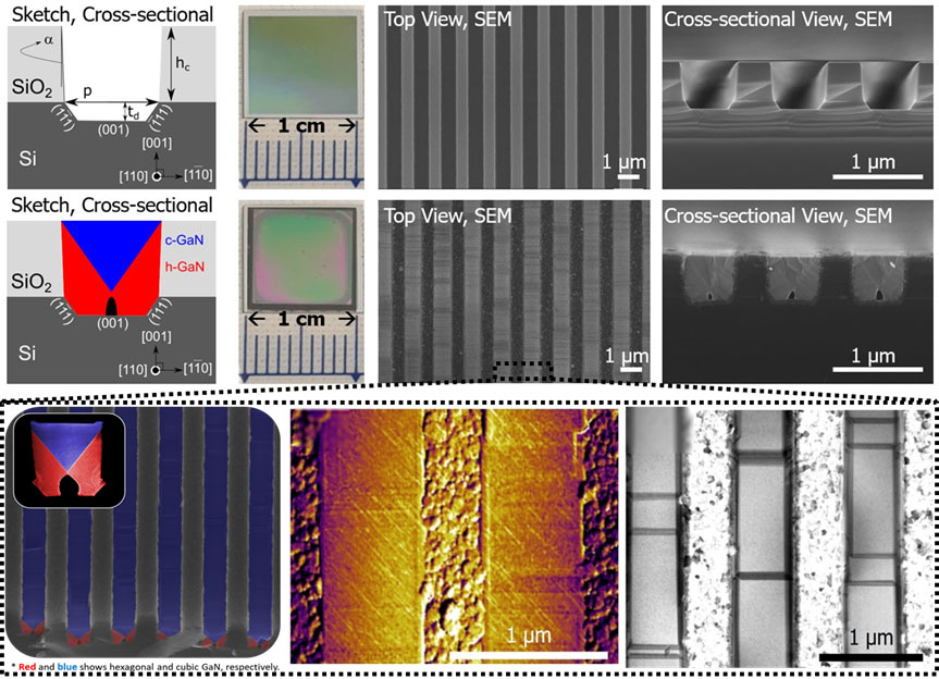
Picture: Cubic GaN epitaxy on large-area (~1cm2) U-grooved silicon (100) dies is demonstrated. (Top row) U-grooved silicon (100) and (middle row) cubic GaN atop (from left to right) Cross-sectional sketches, top-view photographs, top-view SEM images, and cross-sectional view SEM images of. (Bottom row) Cubic GaN structural characterization. (From left to right) Phase-mapping, tapping-mode AFM and bright-field top-view STEM images are shown. The plan-view STEM reveals that no threading dislocations or other types of dislocations on the cubic GaN surface. Stacking faults with a density of 3.27±0.18´104cm-1 are observed.
The researchers study the structural and optical properties and demonstrate, through temperature-dependent and time-resolved photoluminescence measurements, a high as-grown cubic GaN band-edge emission internal quantum efficiency (IQE) of ~26% (25.6%±0.9%).
As well as further identifying the optical defect levels, the researchers report a technique for selective etching of the low-temperature AlN buffer layer, SiO2 sidewalls, and hexagonal-phase GaN. This increases the efficiency to ~32% (31.6%±0.8%), attributed to the decrease in the radiative recombination lifetime via the removal of defective hexagonal-phase GaN. It also points to the potential path of achieving a continuous cubic GaN film.
Overall, the UIUC team reckons that, in reporting cubic GaN on U-grooved silicon with high structural and optical quality, it has demonstrated an encouraging stepping stone for creating next-generation cubic-phase-based III-nitride devices.
Cubic-phase III-nitride LEDs overcome efficiency droop
Efficiency droop halved in cubic- versus hexagonal-phase InGaAlN LEDs


