


News: Microelectronics
13 January 2022
ULTRARAM memory demonstrated on silicon wafers for first time
A type of patented computer memory known as ULTRARAM has been demonstrated on silicon wafers for the first time, representing a step towards its large-scale manufacture (Peter D. Hodgson et al, ‘ULTRARAM: A Low-Energy, High-Endurance, Compound-Semiconductor Memory on Silicon’, Advanced Electronic Materials; DOI: 10.1002/aelm.202101103).
ULTRARAM combines the non-volatility of a data storage memory like flash with the speed, energy efficiency and endurance of a working memory like dynamic random access memory (DRAM). To do this it utilizes the properties of compound semiconductors to yield a non-volatile memory with the potential to achieve fast, ultralow-energy electron storage in a floating gate accessed through a triple-barrier resonant tunneling heterostructure.
Initially patented in the USA, further patents on the technology are currently being progressed in key technology markets around the world. However, Due to the maturity of the silicon chip-making industry and the multi-billion dollar cost of building chip factories, implementation of any digital electronic technology on silicon wafers is essential for its commercialization.
Now, in a collaboration in the UK between the Physics and Engineering Departments at Lancaster University and the Department of Physics at Warwick University, ULTRARAM has been implemented on a silicon substrate for the first time (a vital step towards cost-effective mass production).
“ULTRARAM on silicon is a huge advance for our research, overcoming very significant materials challenges of large crystalline lattice mismatch, the change from elemental to compound semiconductor and differences in thermal contraction,” says professor Manus Hayne of Lancaster’s Department of Physics, who leads the work.
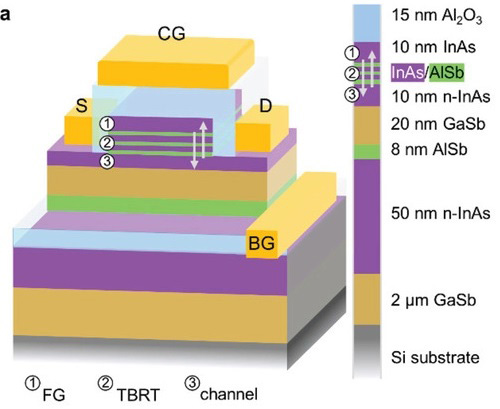 Picture: ULTRARAM device concept: schematic cross-section of a device with corresponding material layers. The floating gate (FG), triple-barrier resonant-tunneling structure (TBRT), and readout channel are highlighted. Arrows indicate the direction of electron flow during program/erase operations.
Sample growth using molecular beam epitaxy (MBE) begins with the deposition of an aluminium antimonide (AlSb) nucleation layer to seed the growth of a gallium antimonide (GaSb) buffer layer, followed by the III–V memory epilayers. Fabricated single-cell memories show clear 0/1 logic-state contrast after ≤10ms duration program/erase pulses of ≈2.5V (a remarkably fast switching speed for 10µm and 20µm devices). Furthermore, the combination of low voltage and small device capacitance per unit area results in a switching energy that is orders of magnitude lower than DRAM and flash, for a given cell size.
Extended testing of devices reveals (extrapolated) data retention (storage) times in excess of 1000 years, fast switching speed (for device size), and degradation-free program-erase cycling endurance of over 107 program/erase cycles (100-1000 times better than flash memory). This performance for ULTRARAM devices on silicon wafers actually surpasses very recent results for similar devices on gallium arsenide (GaAs) compound semiconductor substrates, say the researchers.


