


News: Markets
19 January 2022
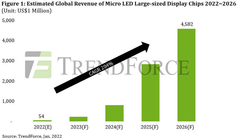
Micro-LED chip market for large-sized displays to grow at 204% CAGR from $54m in 2022 to $4.5bn in 2026
With micro-LED large-sized displays moving towards the home theater and high-end commercial display markets, revenue for micro-LED large-sized display chips will be $54m in 2022 then rise at a compound annual growth rate (CAGR) of 204% to $4.5bn in 2026, forecasts market research firm TrendForce. Technical obstacles will be conquered one by one over time, it adds. The development of micro-LED large-sized displays will peak between 2026 and 2030, and annual revenue for micro-LED chips has the opportunity to reach tens of billions of dollars, reckons the firm.
In recent years, major global brands in various regions have released micro/mini-LED self-emissive large-sized display products, notes TrendForce. The world’s leading TV maker Samsung released a 146-inch TV (‘The Wall’) in 2018 and continues to release 75-inch, 89-inch, 101-inch, 110-inch, 219-inch and 292-inch large tiled wall displays at the Consumer Electronics Show (CES) in Las Vegas each year. Due to the evolution of different application scenarios and technologies, the future development trend of micro-LED large-sized displays will be in home theaters, corporate headquarters, and boutique stores, it is reckoned. Commercial indoor and outdoor large-sized displays are mainly based on mini-LED self-emissive large-sized displays. To satisfy the requirements of close indoor viewing, micro-LED large-sized displays require a theater-level experience, seamless tiled display splicing, pursuit of zero borders, thin design, and competitive pricing. Thus, active matrix (AM) would be the first choice for display design.
Existing micro-LED large-sized displays still face the dual challenges of technology and cost (including micro-LED chip cost) and the three key technologies of backplane technology, driving technology, and the mass transfer process, notes TrendForce.
In terms of micro-LED chip cost, due to the enormous number of chips used and the need for consistent wavelength uniformity to achieve perfect display quality, the cleanroom level requirements for epitaxial and chip processes, control of process conditions, and inspection and maintenance during processes are very strict, greatly increasing the relative process defect rate and overall cost.
In terms of mass transfer, the current mass transfer technologies used in micro-LED large-sized displays include pick-and-place technology and laser transfer technology, each with its own advantages and disadvantages. TrendForce believes that, although existing micro-LED mass transfer technology is still in the product development and adjustment stage, there have been no real quantitative achievements. However, in terms of pick-and-place mass transfer equipment capacity, using 10cm2 transfer stamps to transfer 34µm x 58µm micro-LED chips, production capacity (UPH; unit per hour) is about 7 million units. If the laser mask opening of laser mass transfer technology is 8mm2, production capacity is about 12 million units. No matter which kind of transfer technology, the mass transfer capacity of micro-LED large-sized displays needs to reach at least a 20 million unit level of efficiency and 99.999% yield in the future to meet the conditions for mass commercialization, it is reckoned.
Active-matrix design to aid development of micro-LED technology
In terms of backplane and drive technology, passive-matrix (PM) drive design is based on a PCB backplane with a passive drive circuit structure, using MOSFET as the current-switching element. Therefore, overall structure is more complex and requires a wider placement area for circuit components. In addition, when dot pitch is reduced to less than P0.625, the PCB backplane will encounter the challenges of line-width and line-space mass-production limitations and rising cost. Thus, the existing technological state of the passive-matrix (PM) drive design is more suited to large-sized display applications utilizing dot pitches greater than P0.625 and equipped with a mini-LED. However, for consumer micro-LED TVs employing a dot pitch less than P0.625, active-matrix (AM) drive design will become the new direction of display design, TrendForce says. Since panel manufacturers consider that a TFT glass backplane with LTPS (low-temperature polysilicon) switching technology is mature technology, it is necessary to adjust certain portions of the manufacturing process and parameters to precisely control and drive micro-LED current.
In addition, to achieve seamless tiled display splicing technology, glass metallization and side wire electrode glass will become further technical challenges. As resolution becomes higher and dot pitch is reduced, the front circuit of TFT glass must be guided to the back along the side or by using through-holes. Glass metallization technology then becomes key. Since existing glass metallization technology is still afflicted with technical bottlenecks resulting in high cost due to low yield), when these bottlenecks are resolved with future technology, the launch of mass-production glass metallization will become the advantage of active-matrix backplanes. Future active-matrix (AM) drive design with micro-LED chips and seamless splicing technology have the opportunity to become the mainstream technology for micro-LED TV development and the key to unlocking a new wave of micro-LED large-sized display cost optimization, concludes TrendForce.
Micro-LED chip revenue for TVs to grow at 250% CAGR to $3.4bn in 2025


