


News: Optoelectronics
6 January 2022
VCSEL micro-transfer to silicon nitride PICs
Researchers based in Belgium and Sweden have used micro-transfer printing to integrate 850nm-wavelength vertical-cavity surface-emitting lasers (VCSELs) with silicon nitride (SiNx) photonic integrated circuits (PICs) [Jeroen Goyvaerts et al, Optica, v8, p1573, 2021].
The team from Ghent University-imec in Belgium, Chalmers University of Technology in Sweden, and imec in Belgium see potential for refractive index and biological sensing and power-efficient data-communication applications. The 850nm range has a low water adsorption coefficient. Silicon nitride as a light transmission medium covers the wavelength range 400-2350nm, i.e. visible to near-infrared. By contrast, silicon PICs are restricted to infrared wavelengths longer than 1100nm.
The researchers suggest that the micro-transfer printing approach could overcome the limitations of other approaches in terms of scalable low-cost, large-volume production.
The bottom-emitting VCSELs were fabricated on the III-V epitaxial wafers (Figure 1) before transfer to the SiNx PIC. The top titanium/platinum/gold contacts were mainly reflective disks except for a few test devices with annular contacts allowing light out of the top.
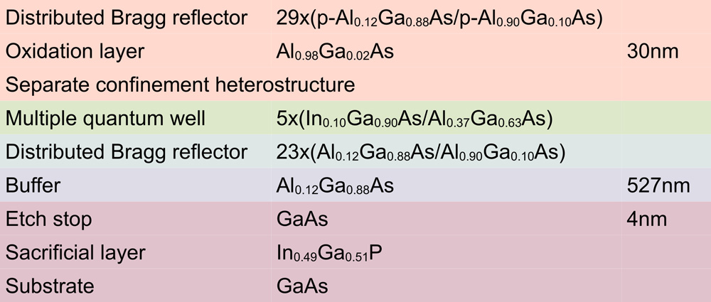
Figure 1: Epitaxial structure for VCSEL.
The top VCSEL mesa was formed by chlorine plasma etch. Silicon nitride was deposited to protect the device from unintentional oxidation. The VCSEL aperture was formed using wet oxidation of an aluminium gallium arsenide (Al0.98Ga0.02As) layer. The aperture diameter was set to less than 5μm with a view to achieving single-mode lasing.
The n-type contact consisted of annealed nickel/germanium/gold. The bottom mesa was created using chlorine plasma etch. The etch process stopped in the middle of a 527nm Al0.12Ga0.88As buffer layer. After depositing more SiNx for protection and insulation, titanium/gold contact pads were formed on the top-emitting test devices.
The VCSELs were prepared for release and transfer by opening the SiNx around the devices and etching the Al0.12Ga0.88As with a wet etch consisting of citric acid and hydrogen peroxide. Then hydrochloric acid was used to etch an indium gallium phosphide (InGaP) release layer. The result was 50μmx90μm VCSELs suspended by photoresist anchors.
The micro-transfer printing used a polydimethylsiloxane (PDMS) stamp to pick up and deposit the VCSELs onto the SiNx PIC. The SiNx PIC platform included a 100nm plasma-enhanced chemical vapor deposition (PECVD) nitride anti-reflective coating. The adhesion of the photoresist around the VCSEL to the stamp depends on the stamp speed: fast for pick-up and slow for target deposition. Bonding of the devices was achieved by spin-coating target substrates with 40nm diluted divinyl-siloxane-benzocyclobutene (DVS-BCB)-mesitylene (1:8).
The fabrication continued with removal of the VCSEL encapsulation, bonding-layer curing, and planarization with DVS-BCB and further curing, followed by reactive-ion etch thinning of the DVS-BCB planarization and creating slanted openings. The etch also removed unwanted SiNx to allow the final step of adding titanium/gold probe contacts.
The VCSELs on SiNx PIC used a diffraction grating to couple the laser light laterally into 300nmx6μm waveguides that tapered down to 550nm to give single-mode transmission to a fiber grating coupler (Figure 2). The peak waveguide-coupled power was 100μmW split into a right and left waveguide. The power in the ‘left’ waveguide was more than 50μmW, while the power in the right was somewhat less. The different power transmission is attributed to misalignment of the printing process.
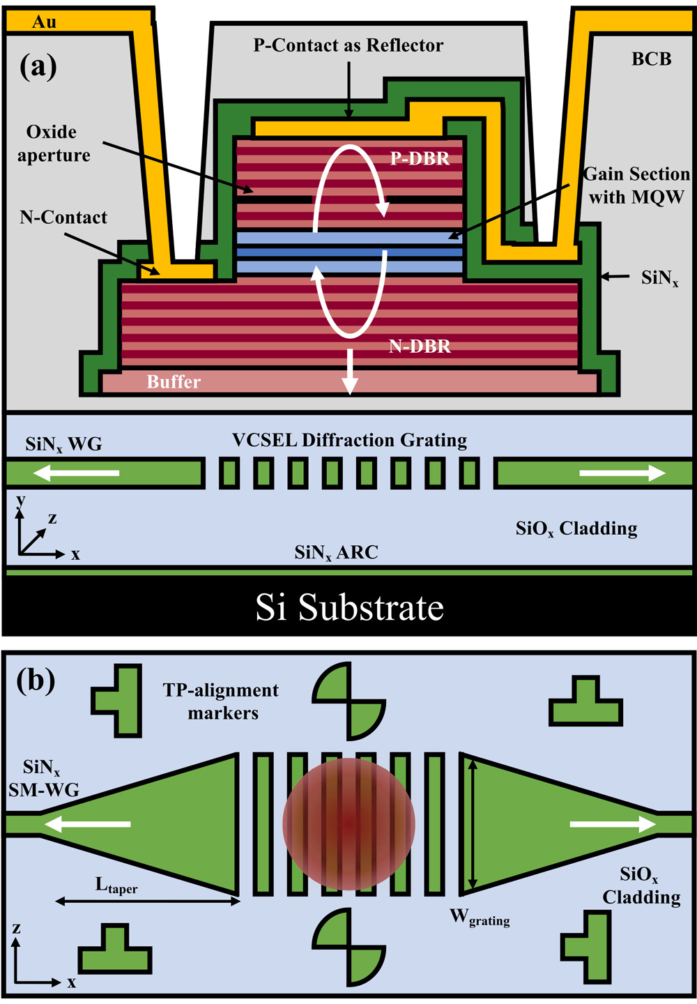
Figure 2: (a) Cross-sectional schematic of micro-transfer-printed vertical-cavity-SiNx-integrated laser (VCSIL) on SiNx bidirectional grating coupler; (b) top-down view.
There was some interference from parasitic reflection at the fiber grating coupler, leading to small oscillation of the light power versus current behavior. Reflectionless couplers would eliminate this effect.
Although the researchers admit that the power is quite low, they see it as adequate for the needs of optical refractive index sensing, writing: “The proposed VCSEL can drive well over 100 refractive index sensors in parallel, in combination with high-responsivity, low-dark-current photodetectors.” The team also sees potential for such sensors in a wearable format.
The optical output/electrical input power ratio was 2.4% with the left-right split being 1.3%-1.1%. The side-mode suppression ratio (SMSR) was 29dB over the bias range. Raising the device temperature to 85°C reduced the light output power by around 50%.
Another device was found to have a wavelength tuning range of 5nm, dependent on self-heating from the current injection (Figure 3). The power of this device in one waveguide wing was 32μmW, while the SMSR was 45dB.
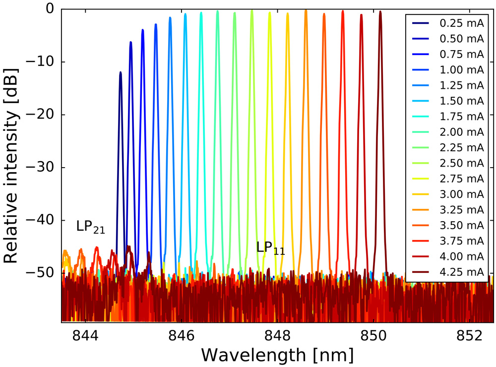
Figure 3: Output spectrum of waveguide-coupled VCSIL. Mode-selective feedback helps to suppress first higher-order LP11 mode with respect to LP21 mode.
A characterization 4μm aperture VCSEL on sapphire demonstrated an output power of 600μmW. The lasing threshold and slope efficiency were 0.16mA and 0.42W/A. The SMSR was 23dB.
VCSELs AlGaAs Silicon nitride PICs
https://doi.org/10.1364/OPTICA.441636
The author Mike Cooke is a freelance technology journalist who has worked in the semiconductor and advanced technology sectors since 1997.


