


News: Suppliers
20 September 2021
Applied Materials launches CMP and hot ion implant systems for 200mm silicon carbide wafer production
Process equipment maker Applied Materials Inc of Santa Clara, CA, USA has announced new products that aimed at helping to enable silicon carbide (SiC) chipmakers to transition from 150mm wafer production to 200mm production. This approximately doubles die output per wafer, helping to satisfy the growing demand for premium electric vehicle (EV) powertrains.
“To fuel the computer revolution, chipmakers moved to ever-larger wafer sizes, dramatically increasing chip output to satisfy burgeoning global demand,” says Sundar Ramamurthy, Group VP & general manager of the ICAPS group at Applied Materials. “Today we are in the early stages of another revolution that will benefit from Applied’s expertise in materials engineering at an industrial scale,” he adds.
“Electrification of the transportation industry is a rising trend, and we are accelerating this inflection point by leading the global transition from silicon to silicon carbide with our Wolfspeed technology,” says Gregg Lowe, president & CEO of SiC materials and device maker Cree Inc of Durham, NC, USA. “Delivering the highest-performing silicon carbide power devices on larger 200mm wafers enables us to increase end-customer value and meet growing demand,” he adds. “Applied’s support in helping speed qualification of 200mm processes in Albany and multi-equipment installations at our Mohawk Valley Fab is expediting this transition,” Lowe says. “Moreover, new technologies being developed by Applied’s ICAPS team, such as hot implant, have broadened and deepened our technical collaboration and helped accelerate our power technology roadmap.”
New 200mm SiC CMP system
SiC wafer surface quality is critically important to SiC device fabrication as any defects on the surface of the wafer will migrate through the subsequent layers. To produce uniform wafers with the highest-quality surfaces, Applied has developed the Mirra Durum CMP (chemical mechanical planarization) system, which integrates polishing, material removal measurement, cleaning and drying in a single system. The new system has demonstrated a 50x reduction in finished wafer surface roughness compared with mechanically grinded SiC wafers and a 3x reduction in roughness compared with batch CMP processing systems.
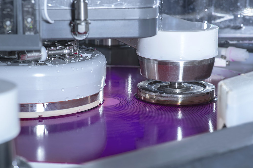
Picture: Applied Materials’ new Mirra Durum CMP system.
Hot implant increases SiC chip performance and power efficiency
During SiC chip fabrication, ion implantation places dopants within the material to help enable and direct the flow of current within the high-power-producing circuits. The density and hardness of SiC material makes it extremely challenging to inject, accurately place and activate the dopants while minimizing damage to the crystal lattice, which reduces performance and power efficiency. Applied has solved this challenge with its new VIISta 900 3D hot ion implant system for 150mm and 200mm SiC wafers. The hot implant technology injects and diffuses ions with minimal damage to the lattice structure, resulting in a more than 40x reduction in resistivity compared with implant at room temperature, it is reckoned.
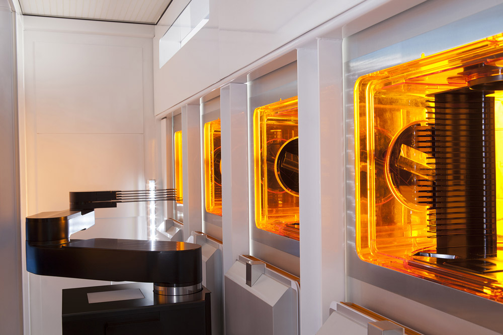
Picture: Applied Materials’ new VIISta 900 3D hot ion implant system.
Applied’s ICAPS (IoT, Communications, Automotive, Power and Sensors) business is developing additional products for the SiC power chip market, including in PVD (physical vapor deposition), CVD (chemical vapor deposition), etch and process control.
Soitec and Applied Materials to jointly develop silicon carbide substrates using Smart Cut technology


