


News: Optoelectronics
25 November 2021
Defect-tolerant type-II QW lasers on silicon
Université de Montpellier and Université Paris-Saclay in France have used ‘type-II’ quantum well (QW) structures to produce extremely dislocation-tolerant III-antimonide interband cascade lasers (ICLs) on silicon substrates [Laurent Cerutti, Optica, v8, p1397, 2021].
One measure of the dislocation tolerance was an estimated 312,000 hour mean time to failure (MTTF) for devices tested under continuous-wave operation at 40°C. The team comments: “To our knowledge, it is the first report of a lifetime longer than 1000 hours for any interband (QW or QD) laser with a density of dislocations above 108/cm2.”
Beyond devices based on gallium antimonide/aluminium antimonide (GaSb-AlSb), the researchers see potential for their type-II QW techniques in other compound semiconductor families, such as indium phosphide, gallium arsenide, or zinc selenide.
III-V light emitters on silicon such as Montpellier/Paris-Saclay’s ~3.5μm ICL are highly desired for integration in silicon photonic integrated circuits (PICs) for interconnects and on-chip sensing.
The usual technique to avoid the performance degradation from threading dislocations is to use localized quantum dots (QDs) to isolate electron-hole recombination into photons from the non-radiative recombination that generally occurs near dislocations and other defects. Even so, lifetimes rapidly reduce when dislocation density exceeds 107/cm2. QW lasers with 5x10⁷/cm2 dislocations have previously achieved a mere 200 hour MTTF.
The non-radiative recombination at dislocations doesn’t just sap device efficiency, it also moves and generates dislocations, a process known as ‘recombination-enhanced defect reaction’, further impeding device performance, pushing it toward failure.
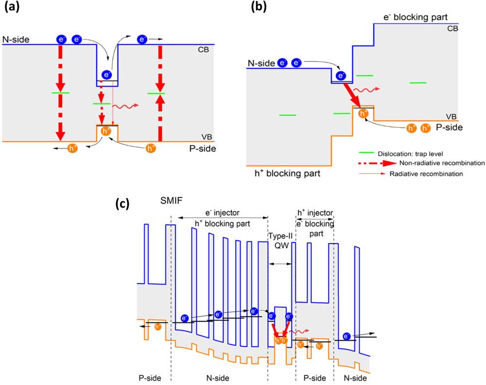
Figure 1: Representations of recombination processes in (a) type-I and (b) type-II QW active regions. (c) Type-II QW ICL with band diagram criteria represented in (b).
The more usual type-I QWs use a band alignment where the electrons and holes gather in a single well (Figure 1). Type-II QW structures instead use separate, neighboring electron and hole QWs. This makes radiative recombination more favorable relative to the mid-gap non-radiative recombination associated with dislocations. Another advantage of the type-II layout is the barrier created to the other carrier type, rather than using the usual separate electron-hole blocking structures to reduce non-radiative recombination in the doped cladding/contact layers.
The Montpellier/Paris-Saclay devices used ICL structures grown by solid-source molecular beam epitaxy on on-axis (001) silicon. The high 13% lattice mismatch with GaSb resulted in a high dislocation density of 1013/cm2. The GaSb buffer was 1.5μm thick. The laser material consisted of 7 IC stages aimed at 3.5μm wavelength emission. The optical confinement was provided by a GaSb separate-confinement heterostructure, along with N-type AlSb/InAs superlattice cladding. The antimonide materials comprised a total thickness of 7.9μm, below the 10μm level where GaSb-based heteroepitaxy on silicon tends to crack.
The researchers comment that most dislocations generated at the GaSb/Si interface were confined within the first 0.5μm growth. By the time the full buffer layer was grown, the dislocation density was in the 8-9x10⁸/cm2 range. The AlSb/InAs superlattice cladding reduced this slightly to ~5x10⁸/cm2 range, still a relatively high level for laser performance.
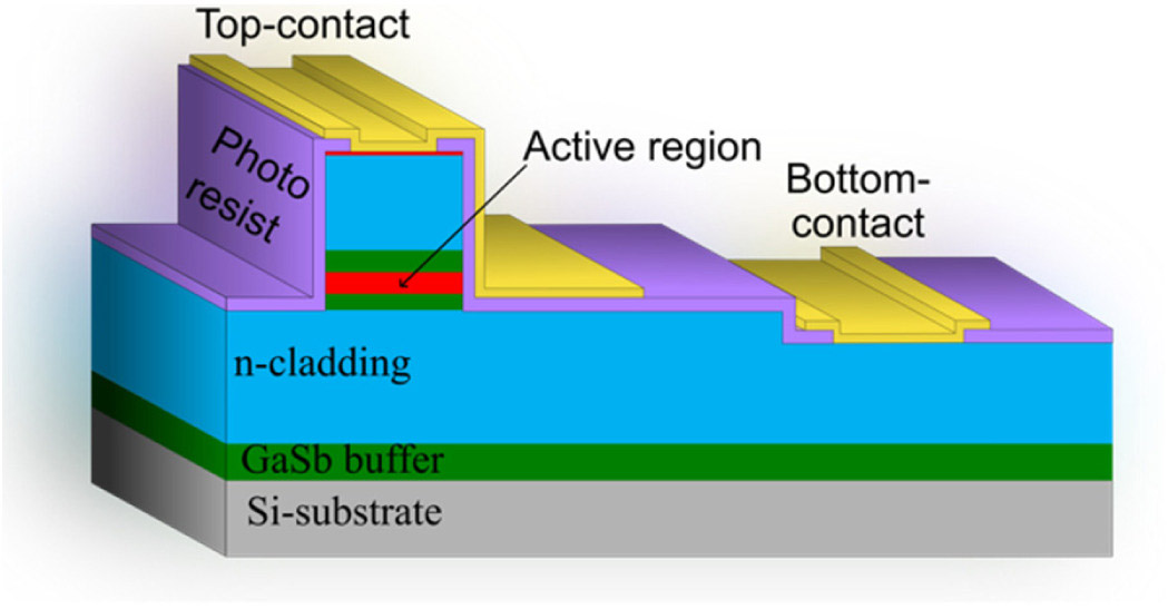
Figure 2: Schematic representation of processed ICL grown on silicon substrate.
The material was processed into 8μm-wide ridge-waveguide laser bars (Figure 2). The cleaved facets were uncoated. The turn-on voltage was around 3V at 20°C, comparable to similar devices produced in the same way on GaSb substrates. The series resistances for 3-1mm cavities were 20-30Ω on silicon, but 1-3Ω on GaSb. The researchers attribute the high resistance on silicon to the “lateral current path and the poor electrical conductivity of the low-doped upper part of the AlSb/InAs bottom cladding layer where this contact is located”.
The laser threshold was in the range 30-70mA, depending on cavity length with similar performances on silicon and GaSb substrates. The output power reached 19mW/facet, and the slope efficiency 0.3W/A.
Below threshold, a 2mm-cavity laser emitted at 3.425μm wavelength with 172nm full-width at half maximum (FWHM). Above threshold, the peak narrowed and red-shifted to 3.436μm.
The increase in threshold with temperature was represented by a characteristic temperature (T0) of 43K between 15°C and 35°C. The shift became more rapid between 40 and 50°C with a reduced T0 of 26K. The thermal performance on GaSb was similar. The multi-mode emission peak also red-shifted from around 3.49μm at 15°C to 3.53μm at 45°C.
To assess long-term reliability, the devices were operated at 40°C and 120mA current injection (~1.5x threshold) and the output power tracked. Periodic threshold measurements were also made (Figure 3). The high operating temperature induced accelerated aging.
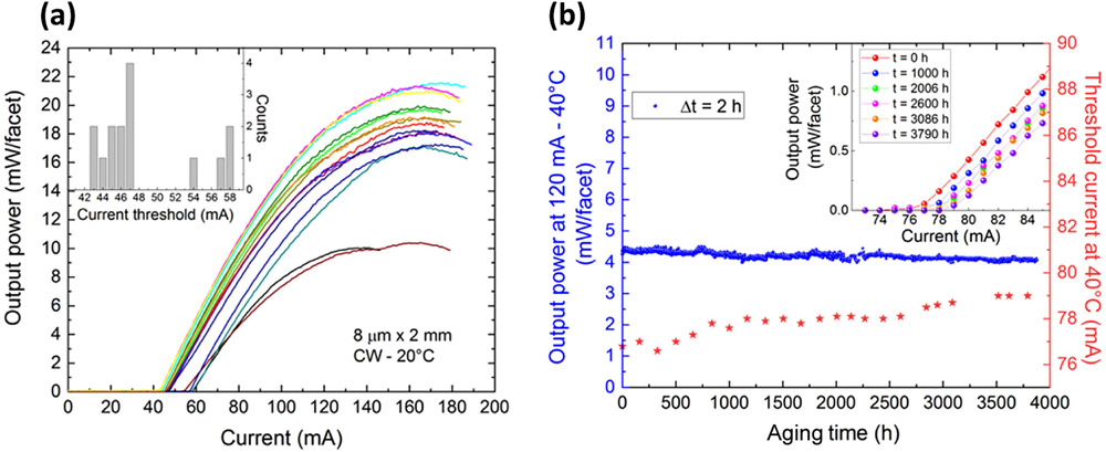
Figure 3: Continuous wave (CW) reliability of ICL grown on silicon. (a) Output power-current (L-I) characteristics of 15 8μmx2mm ICLs tested at 20°C. Inset: histogram of CW threshold current at 20°C. (b) Aging data at 40°C and under 120mA current injection. Inset: L-I characteristics of laser around threshold at different times of aging.
Over 3800 hours, the threshold increased 2.8%, and the output power fell 6.5%. The researchers extrapolate a mean time to failure (MTTF), using a sub-linear data fit, of 312,000 hours, the time needed to double the threshold current.
https://doi.org/10.1364/OPTICA.438272
The author Mike Cooke is a freelance technology journalist who has worked in the semiconductor and advanced technology sectors since 1997.


