


News: Optoelectronics
10 June 2021
Monolithic InGaAs photodetectors on 300mm silicon
IMEC and Ghent University in Belgium claim a record-low dark current density of 1.98x10⁻⁸A/cm2 for indium gallium arsenide (InGaAs) photodetectors monolithically integrated on silicon (Si), using metalorganic vapor-phase selective-area epitaxial growth [Cenk Ibrahim Ozdemir et al, Journal of Lightwave Technology, published online 27 May 2021].
The researchers created a range of nano-ridge waveguide photodetectors (NRWPDs) through selective-area epitaxial growth with aspect-ratio trapping (ART) and nano-ridge engineering (NRE).
The devices promise further III-V integration with the silicon photonics platform in the form possibly of efficient light generation and amplification for future O-band (1260-1360nm) and C-band (1530-1565nm) telecom optical fiber applications. Silicon allows for mass production of optoelectronic components on large-diameter wafers at low cost. But silicon is poor at coupling light and electronics due to its indirect bandgap.
The integration of direct-bandgap materials such as InGaAs has been inhibited by lattice-mismatch problems leading to large defect densities. ART is one method to reduce such defect generation. The IMEC/Ghent work has mainly focused on the shorter 1020nm wavelength range, but IMEC has recently reported NRE InGaAs material growth for operating wavelengths longer than 1200nm, more suitable for silicon and optical fiber photonics.
The 300mm-diameter silicon substrate was n-type doped with ion implantation. Then shallow trenches were formed, 100nm wide and 300nm deep, using a standard ‘shallow trench isolation’ (STI) process from CMOS electronics processing. After oxide planarization, the trenches were further etched with tetramethylammonium hydroxide (TMAH) solution, forming V-shaped bottoms presenting {111} facets of the silicon crystal structure. These facets inhibit anti-phase domains from forming during GaAs epitaxy.
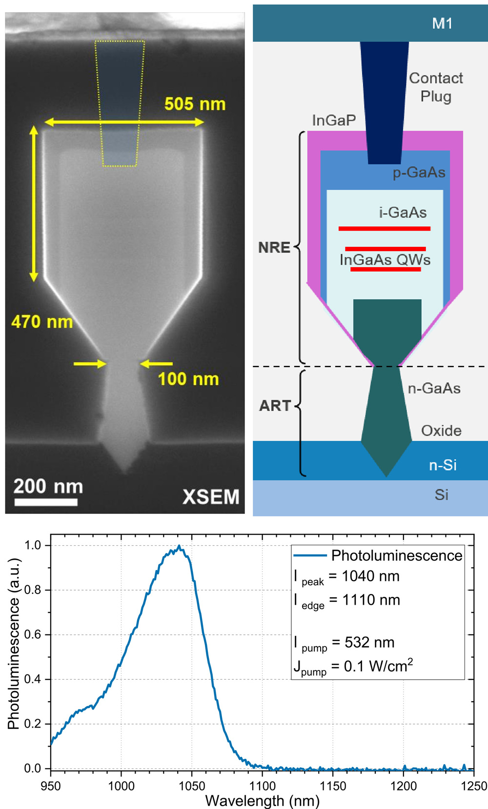
Figure 1: (top left) Cross-section scanning electron microcopy (XSEM) image of GaAs nanoridge with three InGaAs QWs. (top right) Schematic of nano-ridge cross-section. (bottom) Photoluminescence spectrum.
The nano-trenches were filled with n-GaAs via metal-organic vapor phase epitaxy (Figure 1). Misfit dislocations from the GaAs/Si lattice mismatch were trapped in the trench. Above the ART level, the fully relaxed GaAs had a misfit defect density less than 106/cm2.
The active region consisted of three 10nm In0.22Ga0.78As quantum wells (QWs) in GaAs barriers. The device material was completed with p-GaAs contact and InGaP passivation.
The resulting nanoridge waveguide structure was 470nm high and 505nm wide. The ridges were encased in planarized silicon dioxide before tungsten plug contacts were made with the p-GaAs and n-Si layers. Further wiring was added using a standard CMOS copper damascene process.
Photoluminscence experiments show a 1040nm-wavelength peak and 1110nm band edge, consistent with the target composition of the QWs. The nanoridge dimension were chosen to support waveguide modes in this wavelength range for strong optical absorption by the QWs.
The median dark current of 500μm-long devices was 0.05pA at 2V reverse bias and 5fA at 1V (Figure 2). The 5fA value was around the noise floor of the measuring equipment. In terms of current density, the 2V reverse value was 1.98x10⁻⁸A/cm2, described as “the lowest reported dark current for III-V photodetectors monolithically grown on silicon”.
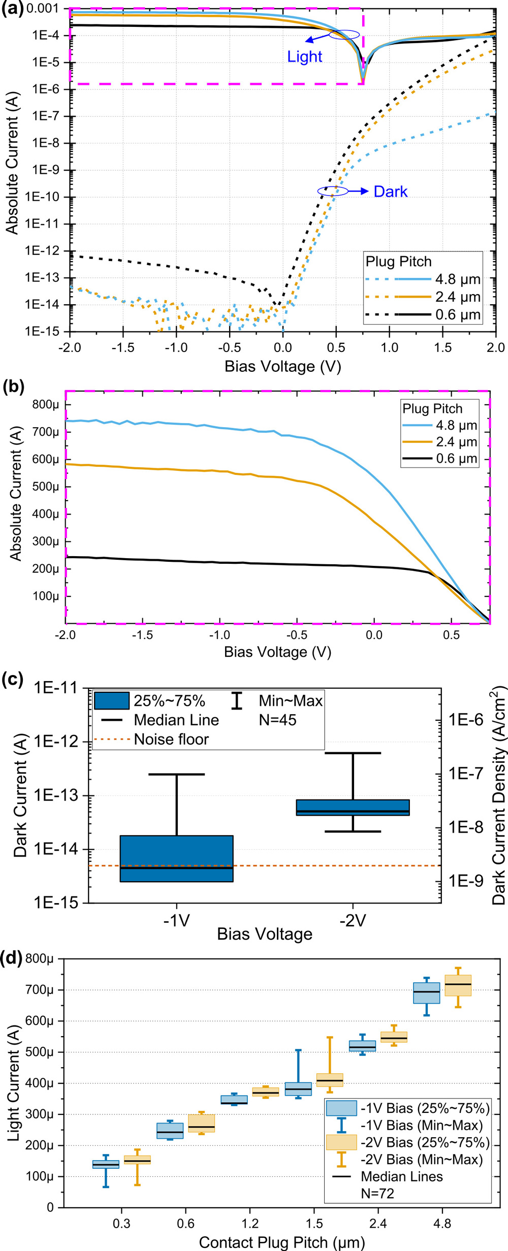
Figure 2: (a) Dark (dash) and light (line) current-voltage curves of devices with different p-contact plug pitches. (b) Light current-voltage zoom-in on linear scale. (c) Dark current statistics at different bias voltages for all devices. (d) Light current statistics of devices with different p-contact plug pitches at different bias voltages, measured at nominal input power.
1020nm laser light was coupled into cleaved-facet devices using active alignment controlled to maximize the photocurrent. While the dark current was found to be independent of the plug placement, the photoresponse did depend of the pitch between the contacts. For a short 0.3μm pitch, the response was ~0.03A/W at 1V reverse bias, but extending the pitch to 4.8μm increased the response to ~0.14A/W.
On the basis of simulations, the researchers suggest “the drop in the internal responsivities for smaller contact pitch values is linked to the loss induced by the optical absorption at the metal contacts.”
Collecting results from devices of various length, the researchers estimate the median internal responsivities and quantum efficiencies of 4.8μm-plug-pitch devices at 0.65A/W and 79%, respectively, at 1V reverse bias. The corresponding values for 2V reverse bias were 0.68A/W and 82%.
The RC bandwidth of the devices was estimated using 1-port S11 measurements from a 50GHz vector network analyzer. Devices with 0.3μm plug pitch and 150μm length had 884Ω series resistance and 91fF junction capacitance at 1V reverse bias, corresponding to an intrinsic RC-limited opto-electrical bandwidth of 1.9GHz. Extrapolating to 4.8μm contact pitch gives a 1.1GHz bandwidth.
The researchers comment: “In future devices, the junction capacitance can be reduced by carefully optimizing the device cross section and eliminating the p-doped GaAs sidewalls, and the series resistance can be reduced by optimizing the contacting and the p-type doping profile.”
Monolithic InGaAs photodetectors Nano-ridge waveguide devices GaAs
https://doi.org/10.1109/JLT.2021.3084324
The author Mike Cooke is a freelance technology journalist who has worked in the semiconductor and advanced technology sectors since 1997.


