


News: Optoelectronics
25 June 2021
C- and L-band microdisk lasers on silicon
Hong Kong University of Science and Technology (HKUST) in China claims the first demonstration of room-temperature continuous-wave lasing of quantum dash (QDash) microdisk lasers (MDLs) on silicon in the C (1530-1565nm) and L (1565-1625nm) optical communication bands [Liying Lin et al, Optics Letters, vol46, p2836, 2021].
The devices were optically pumped, but the researchers believe that electrically pumped MDLs could be realized in the future. QDash light emitters are attractive since they are less affected by crystal defects arising from lattice mismatches between silicon and III-V materials. Also, they are less affected by thermal variations.
The team envisages the realization of multi-channel communication through the fabrication of different diameter and thickness disks on the same substrate with reduced light-source volume and complexity, compared with other laser technologies on silicon. The deployment of electrically driven MDLs on silicon would complete the optoelectronic link between low-cost photonics (waveguides and other structures) and CMOS electronics.
The structure was grown by metal-organic chemical vapor deposition (MOCVD) on an 3.1μm indium phosphide (InP) buffer, which in turn was grown on 1.1μm gallium arsenide (GaAs) that bridged the 8% lattice mismatch with (001) Si. The GaAs layer was subjected to five cycles of thermal cyclic annealing to reduce defects. The InP layer included three sets of 10-period 12nm/4nm In0.63Ga0.37As/InP strained-superlattices designed to reduce defects. The InP was found to be free of anti-phase boundaries, and the surface roughness was only 2.8nm, according to atomic force microscopy (AFM).
The active region consisted of three layers of InAs QDashes in InGaAs. The cladding material was indium aluminium arsenide (InAlAs). The layers were separated by InAlGaAs barriers, creating InGaAs quantum wells in which the QDashes were sited. Photoluminescence spectra showed a peak at ~1.5μm, similar to that of a co-grown structure on an InP substrate. However, the material grown on the native InP demonstrated 3x photoluminescence intensity of that on silicon. The lower intensity leads to the expectation that any laser threshold on silicon would by higher than that on InP.
The laser material was fabricated into mushroom-shaped microdisks with the undercut 500nm to form the 900nm-high stem (Figure 1). The researchers focused on creating smooth sidewalls of the disks, since these were designed to reflect the ~1.5μm light, creating a whispering gallery mode resonance. The undercut trapped the light in these modes rather than allowing leakage into the template of the first radial mode.
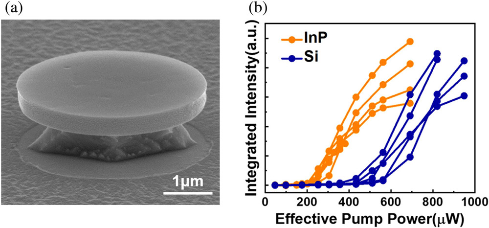
Figure 1: (a) Scanning electron microscope image tilted at 70° of 4μm-diameter microdisk laser. (b) Light intensity versus optical pump power for microdisks on InP and Si, showing thresholds at 200μW and 500μW, respectively.
Continuous-wave pumping on a 3.8μm-diameter 435nm-thick disk produced laser light at 1555nm. Numerical simulations suggest the light came from the transverse electric first radial mode with azimuth mode number 19 (TE19,1). Below threshold a number of peaks were seen in the spectrum, with just one becoming dominant before lasing. The threshold power was as low as 400μW, a value seen as being the lowest reported for such devices so far.
Temperature-dependent studies gave a characteristic T0 for the threshold variation of 65.8K in the range 288-323K. The team comments: “This value is much higher compared with other reported T0 for optically pumped QD MDLs grown on both silicon and III-V native substrates.” The researchers also say that 323K is the highest temperature reported for such devices to lase.
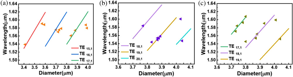
Figure 2: (a)–(c) Experimental data of MDLs with 275–300, 375–400 and 420–440nm membranes, respectively. Lines represent 2D finite difference time-domain (FDTD) simulations based on representative thicknesses of 280, 380 and 435nm accordingly.
Varying the disk diameter between 3.4μm and 4.0μm and the disk thickness between 275nm and 440nm allowed peak wavelength coverage from 1.54μm to 1.61μm, covering the C (1530-1565nm) and L (1565-1625nm) optical communication bands. Optical simulation suggested that different modes were excited in different cases (Figure 2).
Microdisk lasers QDashes InP GaAs InGaAs InAs MOCVD
https://doi.org/10.1364/OL.420106
The author Mike Cooke is a freelance technology journalist who has worked in the semiconductor and advanced technology sectors since 1997.


