


News: LEDs
14 January 2021
Deep UV tunnel-junction LED efficiency
University of Michigan in the USA has reported boosting the efficiency of tunnel-junction deep ultraviolet (UV) light-emitting diodes (LEDs) by one to two orders of magnitude over previous reports on devices operating around 255nm wavelength [A. Pandey et al, Appl. Phys. Lett., vol117, p241101, 2020].
Deep UV LEDs are of much interest for sterilization applications, particularly in these pandemic-ridden times. Apart from healthcare, sterilization capabilities are of interest in the food preparation industry, with a view to avoiding spoilage. Although 260-280nm wavelengths have been the main ones deployed for these purposes up to now, shorter wavelengths may have some advantages in terms of effectiveness.
Creating efficient LEDs at these wavelengths is a challenge that increases as the wavelength shortens. External quantum efficiencies have reached 20% at 275nm, 10% at 265nm, but only 4.5% at 255nm. Asymmetric doping, with hole density and mobility being so much inferior to those of electrons, is one of the major impediments to efficient LEDs based on aluminium gallium nitride (AlGaN) semiconductors.
The Michigan team is looking to tunnel junctions to reduce the dependence of devices on poorly performing p-type conduction. Tunnel junctions allow an n-type component on the hole injection side to improve current spreading, reducing bunching of current density and consequent efficiency droop effects. Before the Michigan report, tunnel-junction devices at 255nm had only managed efficiencies of less than 0.1%.
The heterostructures (Figure 1) for the devices were grown by a molecular beam epitaxy (MBE) system with a radio-frequency plasma-assisted nitrogen source. The AlN-on-sapphire templates were supplied by Japan-based DOWA Holdings Co Ltd. The bottom n-contact layer was annealed in-situ in several steps with a view to improved structural and optical properties.
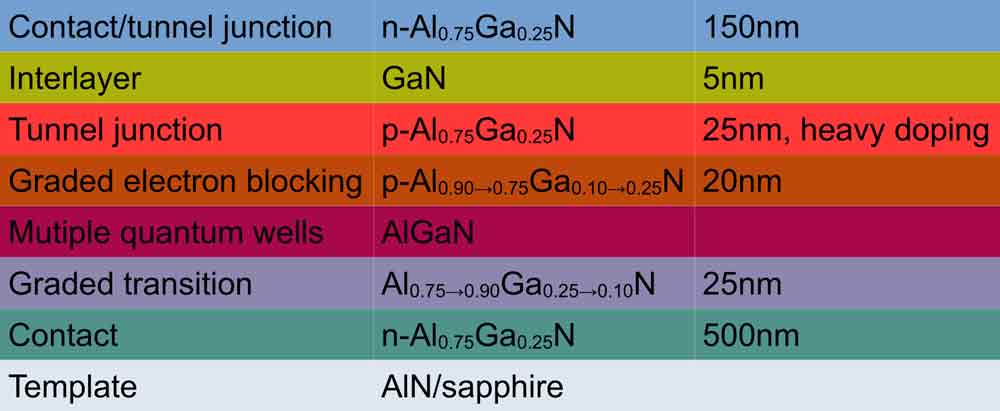
Figure 1: Heterostructure.
The multiple quantum well layers consisted of four AlGaN wells targeted at 255nm-wavelength emission. The thickness of the barrier layers varied, decreasing from 6nm down to 3.5nm. The researchers explain: “Simulations have shown that the reduced barrier thickness closer to the p-doped side of LEDs can help improve device performance by increasing hole injection into the quantum wells, thereby leading to more even charge carrier distribution in the active region.”
The electron-blocking layer was graded to take advantage of the charge polarization of the chemical bonds to give an enhancement of the p-type doping and thus hole injection into the light-emitting region.
The final n-AlGaN component of the tunnel junction included an annealing after 100nm growth. The thin GaN interlayer between the two components of the tunnel junction was designed to reduce the depletion width, enhancing tunneling probability. Again, charge polarization effects at the interfaces between GaN and AlGaN aided this aim.
The MBE used slightly Ga-rich conditions to “enhance dopant incorporation and increase the internal quantum efficiency of AlGaN heterostructures”. At the same time, annealing reduced the tendency of Ga-rich growth to introduce “crystalline defects due to the presence of gallium droplets on the sample surface”. The annealing consisted of raising the temperature by 50°C and shutting off the flow of material into the growth chamber.
The material was fabricated into LEDs with a 30μmx30μm mesa, silicon dioxide passivation, annealed titanium/aluminium/nickel/gold electrodes, and reflective aluminium/gold contact pads (Figure 2). Light was emitted through the sapphire back-side of the LED.
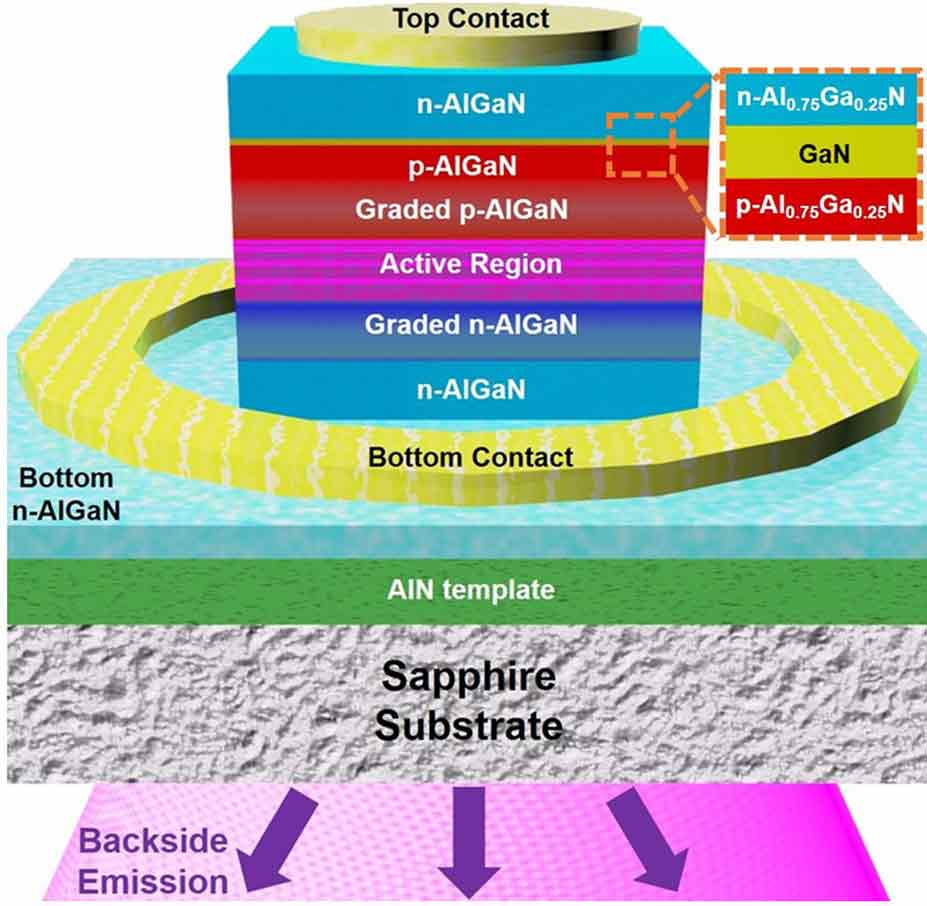
Figure 2: Schematic for tunnel-junction deep UV LED.
The researchers report a sharp turn-on voltage and negligible reverse-bias leakage under continuous wave (CW) injection. “It is noticed that the device has much improved current rectification, compared to previously reported tunne- junction devices emitting at similar wavelengths, due to the reduced leakage current in the present devices,” they comment.
As the current density increased to 200A/cm2, the team saw little variation in the peak emission wavelength, unlike in standard LEDs, which suffer from shifting of the energy levels with applied bias - the ‘quantum-confined Stark effect’. The constancy of the emission peak position “can be explained by the strong charge carrier confinement in the Ga-rich nanoclusters in AlGaN quantum wells grown under slightly Ga-rich conditions by MBE,” the team says.
A significant increase in the full-width at half-maximum (FWHM) of the emission peak on the low-wavelength side “can be explained by luminescence from recombination of carriers within the graded p-doped region of the device”. In other words, the electron-blocking layer is not sufficient in its appointed task of stopping electron carrier overflow.
The external quantum efficiency (EQE) and wall-plug efficiency (WPE) reached 5.3% and 3%, respectively, under CW conditions (Figure 3). “These values are nearly one to two orders of magnitude higher than those of previously reported tunnel-junction devices operating at such short wavelengths,” the researchers report. The team believes better packaging could enhance these efficiencies.
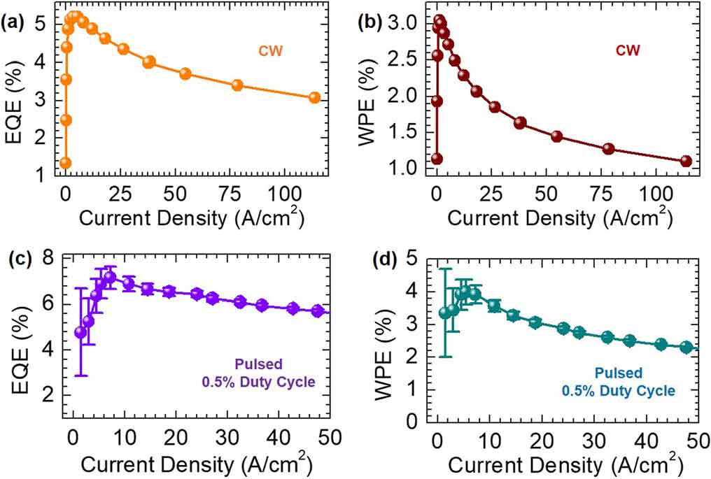
Figure 3: (a) EQE versus current density under CW bias at room temperature. (b) WPE versus current density under CW bias. (c) Pulsed EQE. (d) Pulsed WPE.
The device suffered severe efficiency droop at high current injection, which was not improved by reducing self-heating effects with pulsed injection, although the peak EQE and WPE were enhanced to 7.2% and 4%, respectively. The researchers point to carrier overflow as the suspected main culprit in the droop. This is evidenced by the pulsed injection test and the spectral behavior, along with other recent studies in the academic literature.
UV LEDs MBE AlGaN AlN-on-sapphire templates
https://doi.org/10.1063/5.0036286
www.dowa-electronics.co.jp/semicon/e/epi/index.html
The author Mike Cooke is a freelance technology journalist who has worked in the semiconductor and advanced technology sectors since 1997.


