


News: LEDs
26 August 2021
More evidence for Auger causing GaN LED efficiency droop
University of California Santa Barbara (UCSB) in the USA and Ecole Polytechnique in France have analyzed electron emission spectroscopy (EES) results on indium gallium nitride (InGaN) light-emitting diodes (LEDs), concluding that Auger recombination is the dominant cause of efficiency droop [Wan Ying Ho et al, Appl. Phys. Lett., v119, p051105, 2021].
Efficiency droop is a particular problem in III-nitride LEDs. External quantum efficiency (EQE) tends to peak in the injection current density range of 1-10A/cm2.
The researchers used LED material grown by Seoul VioSys through metal-organic chemical vapor deposition (MOCVD) on patterned sapphire. The structure featured an 8-period quantum well. The p-contact metal consisted of palladium/gold (Pd/Au) with 2257 hexagonal apertures in a honeycomb arrangement. The hexagons had a 3.5μm apothem (perpendicular distance from a side to the center). The metal strips between the apertures were 3μm wide.
EES was enabled by depositing a sub-monolayer of cesium to create a negative electron affinity (NEA). The cesium layer was optimized by monitoring photo-excited electrons from the p-GaN contact layer.
The energy of the emitted electrons was measured using a spherical sector electrostatic analyzer operated in a constant-pass energy mode. The light output power (LOP) was monitored using a photodetector in continuous-wave mode at room temperature. The peak external quantum efficiency was achieved at an injection current density of order 10A/cm2. The EES experiments were made at current densities up to 45A/cm2 in pulse mode to avoid self-heating effects.
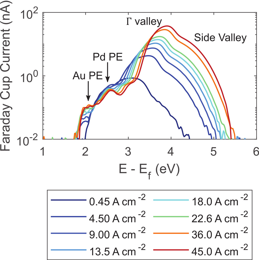
Figure 1: Energy distribution curves from EES experiments.
The researchers attributed a stronger EES signal (Figure 1) than their previous work to using an epitaxial structure with a thinner p-contact region of 20nm p++-AlGaN electron-blocking layer, 20nm p-GaN, and 20nm p++-GaN surface. The EES showed four distinct peaks associated with photoelectric emission from diode-generated light on the Au and Pd contacts, and hot electrons from the main conduction-band valley minimum (Γ) and the first side-valley.
The team reports: “The semiconductor related peaks are one or two orders of magnitude larger than our previous works, which employed thicker p-regions, showing significant improvement in signal-to-noise ratio. This further implied that hot electrons are indeed generated in the bulk region and not by light or other hot-electron generation mechanisms at the surface.”
The researchers see the Au EES signal as constituting an in-situ photometer that should vary linearly with the LOP. Theoretically the LOP should vary as the square of the carrier density (n2) in the MQW, reflecting the two-body electron-hole (eh) recombination process.
The ‘hot-electron’ signal from the side valley is expected to indicate the three-body eeh process where the energy from electron-hole recombination is transferred to an ‘Auger’ electron, rather than a photon. The Auger electron may have enough energy therefore to be trapped in a side valley. A three-body process is expected to vary as the cube of carrier density (n3).
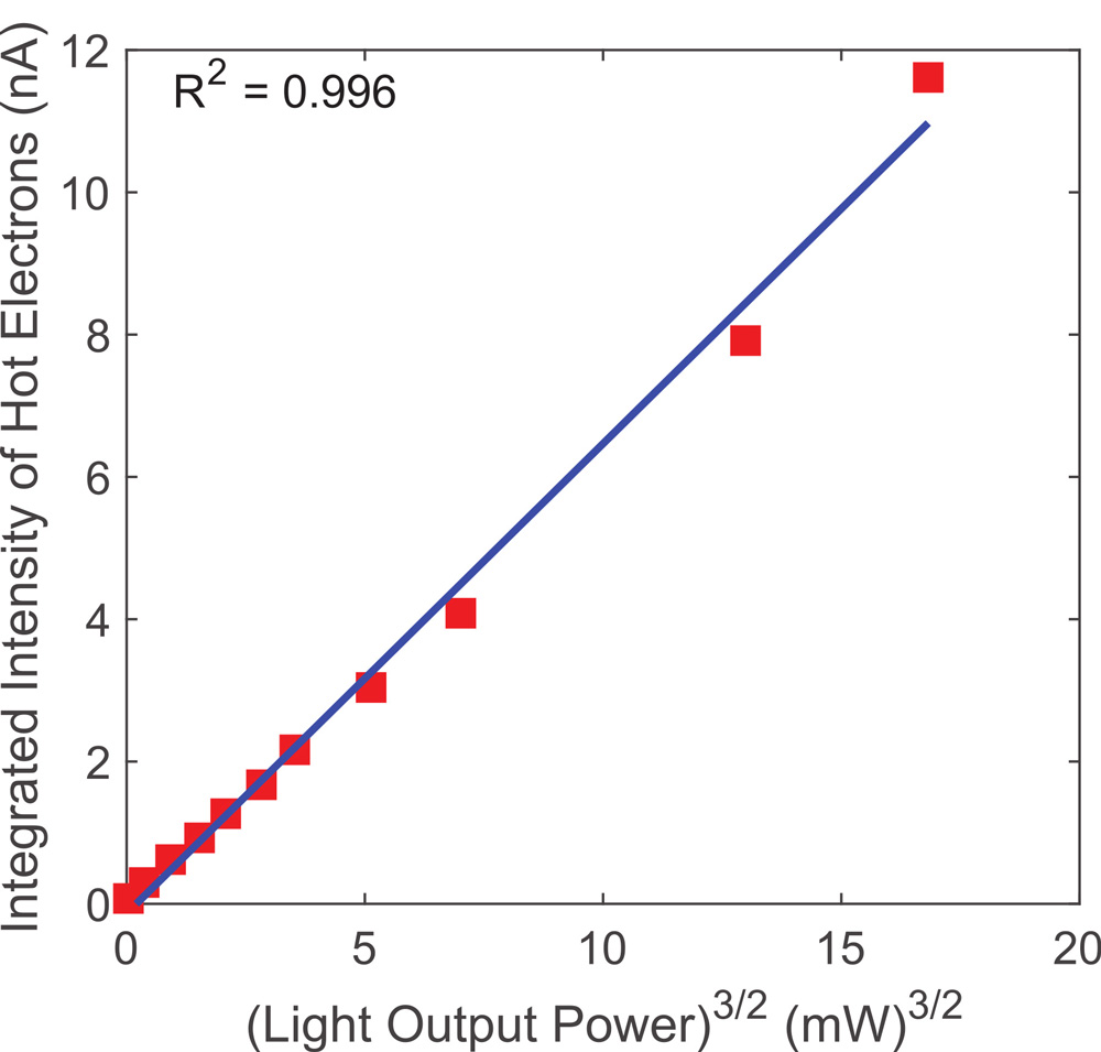
Figure 2: Side-valley peak intensity versus cube of the square root of LOP, and linear fit.
Comparing the two signals would lead one to expect the side valley to vary as LOP3/2 (cube of the square-root), as found experimentally (Figure 2). The main Γ valley signal also is mainly n3, but the fit is improved with the inclusion of a square term, n2, which the researchers suggest is due to trap-assisted Auger recombination (Figure 3).
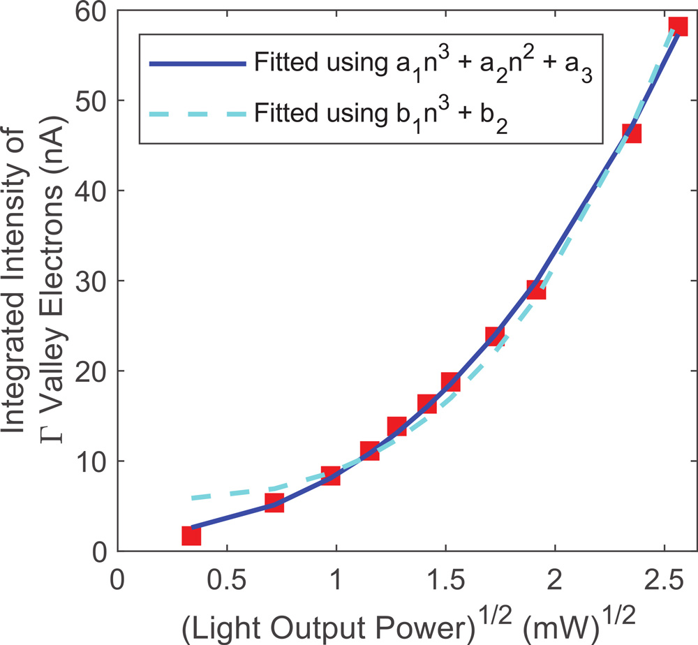
Figure 3: Γ-valley peak intensity versus square-root of LOP.
Alternative explanations of droop as being due to electron overshoot/escape are apparently excluded since the ratio of side valley/Γ-valley signals increases with injection current. Overshoot/escape would lead to the opposite tendency, it is argued. From what I can make out, the overshoot/escape mechanisms should increase the number of Γ electrons, but not side-valley ones.
Auger GaN LEDs GaN LEDs Efficiency droop MOCVD
https://doi.org/10.1063/5.0054636
The author Mike Cooke is a freelance technology journalist who has worked in the semiconductor and advanced technology sectors since 1997.


