


News: Microelectronics
2 August 2021
Transphorm’s joint venture AFSW fab passes from Fujitsu to majority ownership by new partner JCP Capital
Transphorm Inc of Goleta, near Santa Barbara, CA, USA — which designs and manufactures JEDEC- and AEC-Q101-qualified gallium nitride (GaN) field-effect transistors (FETs) for high-voltage power conversion applications — has completed the transaction for its AFSW wafer fab in Aizu Wakamatsu, Japan to be acquired by GaNovation, Transphorm’s joint venture formed recently with its new Palo Alto-based strategic financial partner JCP Capital. The AFSW fab was previously a JV with Fujitsu Semiconductor Ltd (FSL).
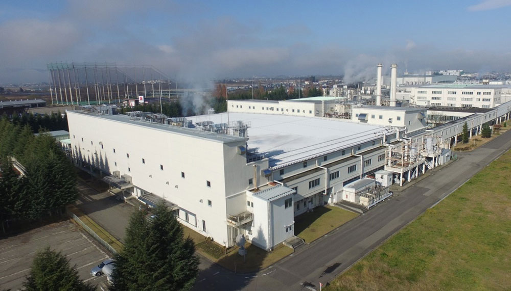
Picture: AFSW wafer fab in Aizu Wakamatsu, Japan.
The transaction completes the previously announced exit of Fujitsu Semiconductor from the AFSW fab. Transphorm’s effective stake in AFSW will be 25% (via its 25% ownership of GaNovation), down from its prior 49% stake. This should reduce Transphorm’s direct capital outlay for AFSW by about 50%, resulting in more efficient profit and loss (P&L), with investment in GaN technologies and applications. In addition, partnering with JCP Capital adds a strategic-financial partner for AFSW that is said to have global strength in the GaN ecosystem, and the shared goal of expanding Transphorm’s GaN power business.
Transphorm stresses that the transition should be seamless for both its customers as well as the existing team and operations at the AFSW fab. With the close of the transaction, FSL’s previously announced exercise of the put option has also been satisfied.
“GaNovation will not only bring significant capital to AFSW, the world’s premier GaN power wafer fab, over the next several years to expand GaN wafer manufacturing, but also contribute to growing the GaN product business together with our portfolio ecosystem at a faster vector, especially in the area of GaN-based fast chargers and adapters,” says JCP Capital founder & managing partner David Cong.
“The partnership with GaNovation and JCP Capital is the ideal next step in Transphorm’s rapid growth and manufacturing of its highest-quality, highest-reliability GaN wafers and products, continuing our asset-light vertically integrated model with strong IP dominance and protection,” says Transphorm’s co-founder & president Primit Parikh. “We also thank Fujitsu Semiconductor for its long-standing partnership as well as its commitment to assist in the successful transition of AFSW going forward,” he adds.
“FSL and AFSW have been working closely with the Transphorm and the JCP Capital team for this transaction that continues forward the strong legacy of semiconductor manufacturing at AFSW,” says commented Kagemasa Magaribuchi, president & representative director, FSL. “Transphorm’s excellence in GaN, with the financial strength brought by JCP Capital, will make AFSW an even stronger manufacturing source for continued success,” he believes. “FSL will also continue to work with AFSW through transition services during the mutually agreed period of time.”
AFSW is believed to be the only GaN-on-silicon foundry that has reported defect densities for GaN-on-Si high-voltage devices that are similar to that of silicon CMOS/bipolar technologies running in the same wafer fab. Transphorm claims that, for its GaN products (including the latest generations such as SuperGaN), this has resulted in demonstrated performance advantage compared with other enhancement-mode (E-mode) GaN products for chargers/adapters in lower-power applications from 45W to several 100W and against other GaN and SiC products for higher-power applications to 10kW.
AFSW is expected to continue to scale as the foundry center of excellence for GaN wafer fabrication while maintaining its ability for existing silicon wafer fabrication.


