


- News
26 September 2019
Silver nanoparticle boost to gallium nitride red light-emitting diodes
Osaka University in Japan has combined silver nanoparticles (Ag NPs) with europium-doped gallium nitride (GaN:Eu) light-emitting diodes to boost red electroluminescence by a factor of two [Jun Tatebayashi et al Appl. Phys. Express, vol12, p095003, 2019]. The output power enhancement is attributed to coupling between local surface plasmon (LSP) free-electron oscillations on the Ag NPs and electron transitions in the Eu ions that produce red photons.
The GaN:Eu LEDs operate through ~620nm-wavelength transitions in the electronic state of the Eu3+ ions, rather than the band-to-band transitions of indium gallium nitride (InGaN) devices, for which ~520nm green wavelengths are a struggle to obtain efficiently.
The research team points out that stable, narrow-wavelength GaN:Eu red LEDs “have recently reached output-powers respectable for commercialization.” They suggest that further performance enhancements could lead to applications such as in micro-LED displays with red, green and blue emitters on a common GaN platform.
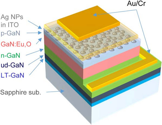
Figure 1: Schematic of fabricated LEDs.
The GaN layers were applied using metal-organic vapor phase epitaxy (MOVPE) on sapphire via trimethyl-gallium and ammonia precursors (Figure 1). The GaN:Eu,O co-doped layer used in addition bis(n-propyl-tetramethyl-cyclopentadienyl)europium (EuCppm2) and argon-diluted O2 sources. The n- and p-type silicon and magnesium doping was achieved by adding monomethylsilane and bis(cyclopentadienyl)-magnesium (Cp2Mg), respectively.
The growth sequence was: 530°C GaN buffer, 1.5μm 1200°C undoped GaN, 2.4μm n-GaN contact, 100nm 960°C GaN:Eu,O active layer, and 1050°C p-GaN contact.
Further processing consisted of 10-minute 800°C annealing in nitrogen to activate the p-GaN doping, formation of self-assembled Ag nanoparticles, 150nm indium tin oxide (ITO) sputtered p-contact, and chromium/gold (Cr/Au) metal contact electron-beam deposition.
Inductively coupled plasma etch was used to expose the n-GaN layer for the metal contact deposition. The final devices were 1mmx1mm in lateral dimensions.
The nanoparticle formation consisted of electron-beam deposition of a silver film, followed by annealing at 200°C for 30 minutes in nitrogen.
Photoluminescence (PL) experiments on the epitaxial material with Ag NPs showed a 622.4nm peak at room temperature. The peak shifted to 621.8nm at 10K. The emission was attributed to 5D0–7F2 transitions in the Eu. At 10K, there are also “several” lesser peaks either side of the main one. [I see two (with a broad ~10nm hump on the short-wavelength side) in the image in the paper, but maybe these break up into “several” at higher resolution.] These peaks become less clearly defined at room temperature. The different peaks are attributed to variations in the electromagnetic environment of the Eu3+ ions in the GaN crystal structure.
“This is a result of the existence of defects such as Ga and N vacancies, as well as carbon, oxygen and hydrogen, yielding various ‘Eu incorporation sites’, and also modifies the transition probabilities of each Eu site,” the team explains.
The intensity of the emissions generally increased with the thickness of the Ag film used to create the NPs – at 20nm the intensity was 3.4x that for the bare material at room temperature (6.65x at 10K). There was a slight intensity dip initially with 5nm Ag, before enhancements set in with thicker Ag films.
The researchers comment: “The observed enhancement of the luminescence intensity is predominantly a result of coupling of the Eu3+ luminescence to the LSP modes of Ag NPs, although a small increase due to reflection at the GaN/Ag NPs interface might be expected after the formation of Ag NPs.”
The PL studies did not show near-band-edge emissions from the GaN material (in the near ultraviolet) or ‘yellow luminescence’ associated with crystal defects. The team writes: “This indicates that electron-hole pairs generated in the GaN host can be efficiently captured to the trap level responsible for energy transfer from the host material to the Eu3+ ion.”
Time-resolved PL analysis at 10K found that the decay time with 20nm Ag NPs was shorter than that for bare material – 204μs, compared with 263μs. The 1.3 increased decay probability was taken as deriving from the coupling between the Eu ions and the LSPs of the Ag NPs. In fact, the decay time was minimized at 194μs with NPs created with 15nm Ag films. The researchers tentatively attribute the increase with 20nm Ag to “the irregular shape and large size variation” of the NPs reducing the coupling with the Eu ions.
The LSP-ion coupling is seen as being rather small, compared with conventional indium gallium nitride (InGaN) quantum well and surface plasmon structures reported in the scientific literature. The researchers suggest that this is due to the much thicker GaN:Eu,O layer, compared with quantum wells – 100nm versus 1-3nm, typically.
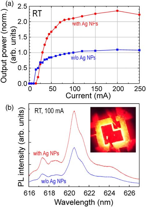
Figure 2: (a) Output-power versus injection current of fabricated GaN-Eu-based LEDs with and without Ag NPs. (b) EL spectra of GaN:Eu-based LEDs under 100mA injection current. Inset shows microscopic image of red LEDs.
Electroluminescence performance was assessed for radiation extracted out of the sapphire back-side of the device (Figure 2). The onset of light emission came at around 10mA current injection. The researchers say that optimization of the thickness and doping density of the p-GaN layer is required to reduce current leakage while maintaining coupling efficiency between the LSP and GaN:Eu layers. The light output saturated around 100mA. The device with Ag NPs had 2.1x the output without the particles at 100mA.
While it is tempting to increase the emission by increasing the Eu concentration, this runs the risk of reducing crystal quality and thus the light emission performance.
Red LEDs GaN InGaN Ag NPs GaN:Eu MOVPE
https://doi.org/10.7567/1882-0786/ab37b0
The author Mike Cooke is a freelance technology journalist who has worked in the semiconductor and advanced technology sectors since 1997.


