


- News
14 November 2019
Improving metal-organic growth of aluminium nitride on silicon carbide
University of California Santa Barbara (UCSB) in the USA have improved metal-organic chemical vapor deposition (MOCVD) aluminium nitride (AlN) growth on silicon carbide (SiC) with a view to aluminium gallium nitride (AlGaN) deep-ultraviolet light-emitting diode (DUV LED) and optoelectronics fabrication [Christian J. Zollner et al, Appl. Phys. Lett., vol115, p161101, 2019].
The work was aimed at providing crack-free AlN templates for AlGaN growth with low threading dislocation density without using costly and time-consuming approaches such as pulsed lateral overgrowth or growing very thick (>10μm) buffer layers.
The researchers comment: “Combining overall improvements in AlN MOCVD techniques, improved SiC wafer quality, and growth-mode control concepts demonstrated in molecular beam epitaxy (MBE), we find that MOCVD growth of AlN/SiC is a viable route to high-quality UV-LED template layers.”
The team also points out that there are highly selective dry etch techniques for efficient SiC substrate removal, raising the prospect of high-efficiency deep-UV LED fabrication. Such removal would be necessary for sub-300nm deep-UV wavelengths that include the UV-C 260nm-285nm range, since SiC is highly absorbing of these high-energy photons. In fact, SiC becomes absorbing around 380nm. UV-C LEDs could be used to kill bacterial and viral pathogens in air, water, and on surfaces.
AlN can also be grown on much lower-cost sapphire, which is transparent to deep UV. The advantage of SiC is that it is a much better match in terms of crystal structure. The researchers also point out that “there is no risk of inadvertent nitrogen-polar growth on the substrate’s Si-face.”
At present, deep-UV LEDs exhibit low wall-plug efficiency due to a number on factors, one of which is the presence of threading dislocations that direct electric energy into non-radiative recombination processes.
The UCSB MOCVD used trimethyl-aluminium and ammonia precursors as the sources of the aluminium and nitrogen, respectively. A 250nm AlN initiation layer was grown at 1200°C, followed by 2.7μm AlN at 1400°C. The growth rates were 1.5Å/s and 6Å/s, respectively. The two-step process targeted reduced numbers of threading dislocations and a smoother surface.
The 4H SiC substrates came from two suppliers. The ‘sample A’ substrate was mechanically polished with polishing marks obscuring the atomic steps typically produced during the crystal growth process. In ‘sample B’, which had a smoother surface from chemical-mechanical planarization (CMP), these steps were visible in terraced surface structures. Samples A and B were 250μm and 500μm thick, respectively.
AlN films grown on sample B were found to have reduced tensile stress and less cracking. “The marked reduction in tension when switching to smooth substrates suggests that small island size is a primary driver of stress generation on rough substrates,” the team comments.
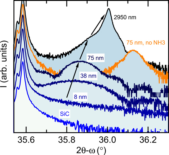
Figure 1: Symmetric triple-axis 2ω-θ x-ray diffraction scans of AlN/SiC films, with SiC double-peak (blue) for reference. Growth sequence with (black) and without (orange) ammonia pretreatment compared up to 75nm, along with full 2.95μm AlN thickness template (black). Logarithmic intensity scale.
A 10 minute ammonia pretreatment of sample B at 1400°C for 10 minutes changed the slight tensile stress to strong compression with a value of -1.1GPa. The surface was also crack-free up to a 5μm scale. X-ray rocking curves also showed reduced full-width at half-maximum (FWHM) diffraction peaks, suggesting higher film quality (Figure 1).
One effect of the pretreatment was to increase the spacing of the atomic steps from 165nm to 330nm. The shorter step distance in the initial surface has been found to increase threading dislocation density and to create lattice stacking mismatch problems.
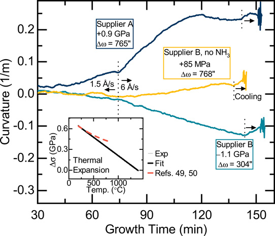
Figure 2: In-situ curvature of AlN template on three substrate types: rough SiC with ammonia pretreatment (top, tensile), smooth substrate (middle, weakly tensile), and smooth substrate with ammonia treatment (bottom, highly compressive). Growth stress and 20-21 FWHM, Δω, listed. Inset: thermal expansion mismatch stress: data (gray) compared with literature models (red, dashed) and linear least squares fit (black, solid).
Laser monitoring of the substrate curvature during growth (Figure 2) suggested a thermal expansion coefficient mismatch in sample B of 1.13x10⁻⁶/°C, which resulted in a slight lattice mismatch increase of 0.15% at 1375°C. A thick AlN layer is fully relaxed at its growth temperature, but on cooling to room temperature develops tensile stress ~700MPa that can lead to cracking.
Plan-view transmission electron microscopy gave a threading dislocation density value of 2.4x10⁸/cm2.
Ammonia pretreatment DUV LEDs MOCVD AlGaN SiC
https://doi.org/10.1063/1.5123623
The author Mike Cooke is a freelance technology journalist who has worked in the semiconductor and advanced technology sectors since 1997.


