


- News
11 June 2019
EVG launches HERCULES NIL 300mm fully integrated lithography track system
EV Group of St Florian, Austria – a supplier of wafer bonding and lithography equipment for semiconductor, micro-electro-mechanical systems (MEMS) and nanotechnology applications – has unveiled the HERCULES NIL 300mm - a fully integrated track system that combines cleaning, resist coating and baking pre-processing steps with EVG’s proprietary SmartNIL wafer-level nanoimprint lithography (NIL) process in a single platform for wafers up to 300mm in diameter.
The HERCULES NIL 300mm is a highly versatile platform designed for companies targeting high-volume manufacturing (HVM). It is the first NIL system based on EVG’s fully modular equipment platforms with swappable modules to give users maximum freedom to configure their systems to best meet their production needs, including bridge capabilities for 200mm and 300mm wafers. EVG’s SmartNIL technology has also been improved and modularized for the HERCULES NIL 300mm, providing what are claimed to be the most advanced nanoimprint capabilities on the market with low-force and conformal imprinting, fast high-power exposure and smooth stamp detachment.
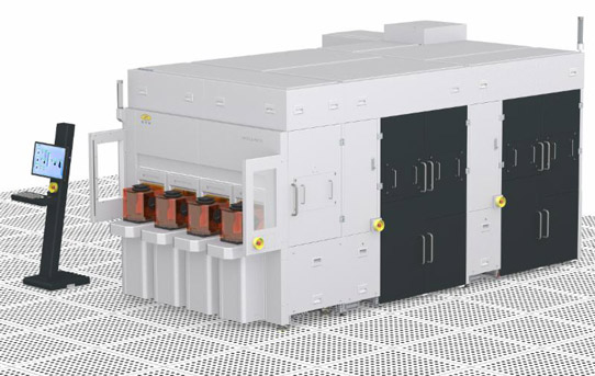
Photograph: HERCULES NIL 300mm fully modular and integrated SmartNIL UV-NIL system.
The HERCULES NIL 300mm supports the production of a variety of devices and applications, including optical devices for augmented/virtual reality (AR/VR) headsets, 3D sensors, bio-medical devices, nanophotonics and plasmonics. Demonstrations of the new system are now available at EVG’s NILPhotonics Competence Center. The firm has already received multiple orders for the new system.
Fulfilling potential of nanoimprint lithography
NIL has proven to be a highly efficient method to fabricate micro- and nanopatterns on large areas, to replicate complex structures and to directly pattern functional layers for a wide range of structure sizes and shapes, says EVG. As a result, NIL is increasingly becoming a key enabling technology to support the production of new devices and applications across a wide range of markets, particularly in photonics and biotechnology. As demand for NIL-enabled devices and applications continues to grow, NIL solutions must be capable of scaling up to higher levels of productivity while maintaining low cost of ownership, adds the firm. SmartNIL technology is the result of years of research, development and field experience to address nanopatterning requirements that cannot be supported by conventional lithography, and has been field proven to be easily scalable from die-level sample sizes all the way up to large-area substrates.
“The HERCULES NIL 300mm represents a major leap forward in bringing SmartNIL to high-volume, wafer-level manufacturing,” believes executive technology director Paul Lindner. “The platform has literally been built from the ground up for high productivity and to provide customers with a high degree of flexibility to support their evolving production needs. For more than 20 years, EV Group has pioneered NIL technology, and today we have the dominant market share worldwide,” he adds. “We work in close collaboration with our customers to ensure their success in implementing NIL in their manufacturing strategy and to provide them with the best possible solution to meet their needs. An example of this is our NILPhotonics Competence Center, which reduces the entry barrier for nanoimprinting and gives easy access to a world-class infrastructure and nanoimprint experts.”
Key attributes of the HERCULES NIL 300mm include:
- fully automated UV-NIL imprinting and low-force detachment;
- processing substrates up to 300mm in diameter;
- fully modular platform that can accommodate up to eight swappable process modules (imprinting and pre-processing), for higher tool productivity;
- 200mm/300mm bridge-tool capability (providing greater flexibility and longer tool lifetime);
- full-area imprint coverage (which avoids pattern stitching errors associated with step-and-repeat lithography systems due to limited field size);
- volume manufacturing of structures down to 40nm and smaller;
- supports a wide range of structure sizes and shapes (including 3D);
- can be used on high-topography (rough) surfaces;
- ability to replicate multiple-use soft stamps to extend the lifetime of master imprint templates; and
- equipped with front-end module with up to four load ports (300mm FOUPs/200mm open cassettes) for continuous operation.
EVG ramps nanoimprint lithography into high-volume manufacturing with HERCULES NIL track system
EVG establishes NILPhotonics Competence Center
www.evgroup.com/en/products/lithography/nanoimprint_systems


